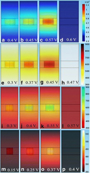
Fig. 18.

Calculated temperature maps extracted from the electro thermal simulations for applied voltages a 0.4 V, b 0.45 V, c 0.575 V, and d 0.6 V for sample P (500 °C annealed); e 0.3 V, f 0.375 V, g 0.45 V, and h 0.475 V for sample Q (400 °C annealed); i 0.3 V, j 0.4 V, k 0.55 V, and l 0.575 V for sample R (300 °C annealed); m 0.15 V, n 0.25 V, o 0.375 V, and p 0.4 V for sample S (200 °C annealed) across the CF geometry of length tox = 20 nm. Different bias points are considered for the devices so that the reset transition for each device can be visualized easily [185]
