
Figure 2.
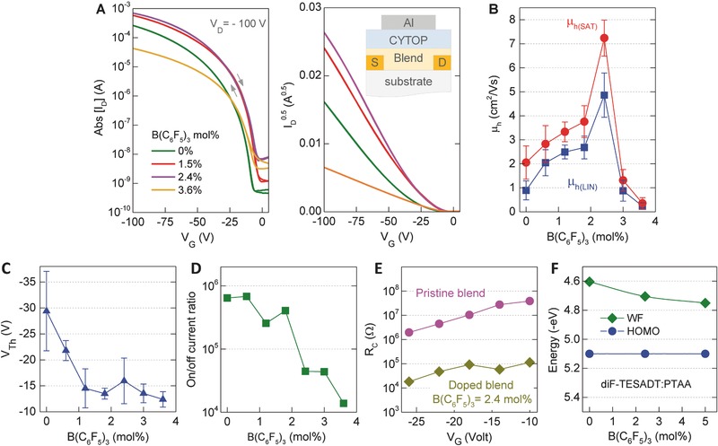
a) Transfer characteristics and corresponding I D 1/2 versus V G plots measured for top‐gate, bottom‐contact diF‐TESADT:PTAA transistors with different B(C6F5)3 concentrations in the range 0–3.6 mol%. Inset shows the top‐gate, bottom‐contact transistor architecture employed. b) Evolution of hole mobility (µ h) as a function of B(C6F5)3 concentration. Panels (c) and (d) display the evolution of threshold voltage (V Th) and current on–off ratio, respectively, as a function of B(C6F5)3 concentration. e) Evolution of contact resistance (R C) versus V G calculated for the pristine and B(C6F5)3(2.4 mol%)‐doped diF‐TESADT:PTAA OTFTs. f) Work function (ϕ) and HOMO energy of the pristine and B(C6F5)3‐doped diF‐TESADT:PTAA blend layers measured by KP and APS, respectively.