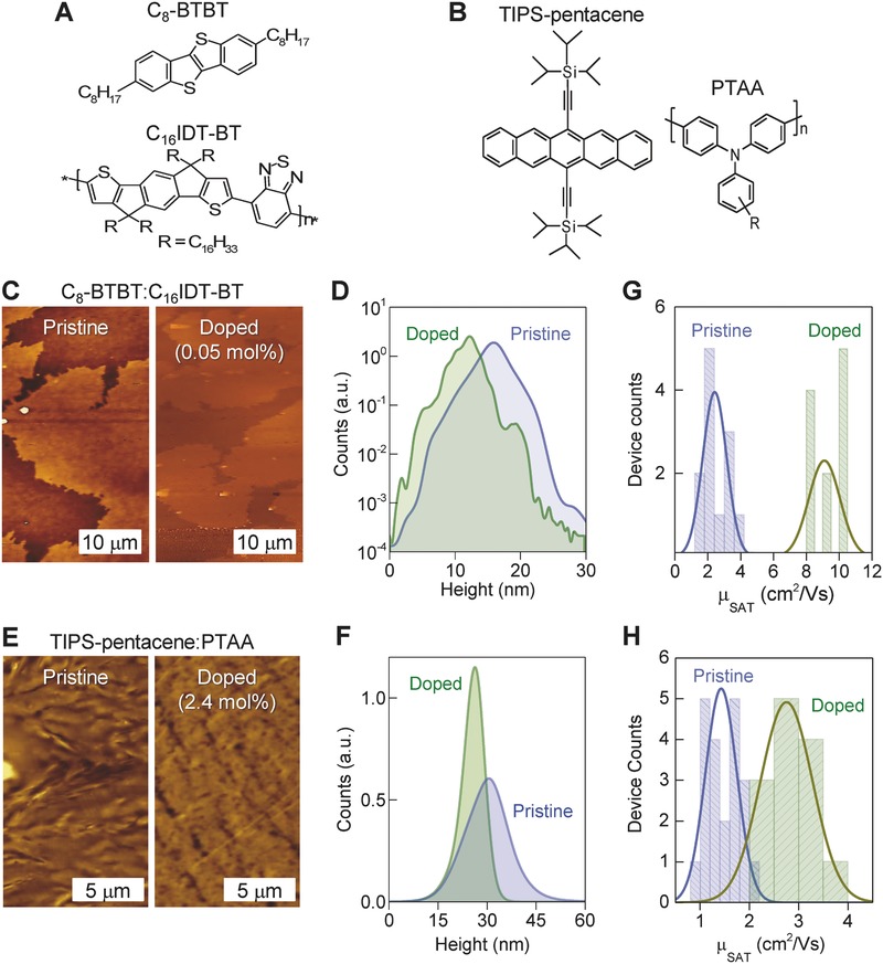
Figure 5.

a,b) Chemical structures of the materials used in the two additional semiconducting blends. c) Topography AFM images of the pristine (0 mol%) and B(C6F5)3‐doped (0.05 mol%) layers composed of C8‐BTBT:C16IDT‐BT and d) the corresponding height histograms. e) Topography AFM images of the pristine (0 mol%) and B(C6F5)3‐doped (2.4 mol%) TIPS‐pentacene:PTAA layers and f) the corresponding height histograms. Panels (g) and (h) show the extracted field‐effect hole mobility measured in saturation (µSAT), for the pristine and B(C6F5)3‐doped C8‐BTBT:C16IDT‐BT (g) and TIPS‐pentacene:PTAA (h) transistors.
