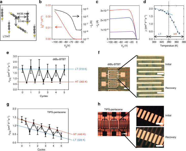
Fig. 6.
Electronic properties and function memory effect of thin film transistors. a Calculated charge transfer integrals in the LT and HT forms of ditBu-BTBT. b Transfer curve in the saturation regime (Vd = −100 V), c output curve and d temperature-dependent apparent mobility in the saturation regime for ditBu-BTBT OFETs. The dashed line indicates the transition temperature at the intersection of the two slopes. Data points are in 5 K increments e Reversible switching of apparent mobility of ditBu-BTBT thin film devices over five thermal cycles. Each mobility value is an average of four devices. Each error bar is calculated from the standard deviation of four devices. f Preservation of thin film morphology and device structure before and after a thermal cycle in ditBu-BTBT. Scale bar on the left corresponds to 500 µm, and the scale bars on the zoomed in images correspond to 100 µm. g Reversible switching of apparent mobility of TIPS-pentacene thin film devices over five thermal cycles. Each mobility value is an average of four devices. Each error bar is calculated from the standard deviation of four devices. h Preservation of thin film morphology and device structure before and after a thermal cycle in TIPS-pentacene. Scale bar on the left corresponds to 500 µm, and the scale bars on the zoomed in images correspond to 100 µm

