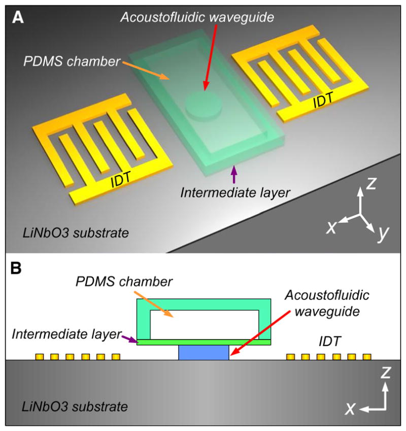
Fig. 1.

a 3D schematic and b 2D view of the acoustofluidic waveguide configuration within the x–z plane. The waveguide sits between the LiNbO3 substrate and the upper microfluidic chamber. An ultrathin intermediate layer was introduced to connect the waveguide and the chamber. The waveguide, chamber, and intermediate layer were made of PDMS in our case studies. A pair of IDTs was placed on both sides of the waveguide, acting as the excitation source to generate the SAWs that travel along the LiNbO3 substrate. The acoustic waves were guided through the waveguide and then transmitted into the fluidic chamber
