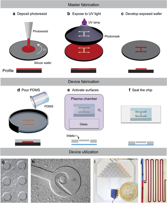
Figure 1.
Fabrication of microfluidic devices. A common method to make microfluidic devices is to make a master by photolithography, which is then used to mold PDMS silicone. (a) Deposition of photoresist on a silicon or glass wafer. The thickness of the photoresist is defined by spinning the wafer at a certain rotational speed for a certain time. (b) UV light exposure through mask. UV light illuminates the desired pattern through a photomask and catalyses photoresist crosslinking. (c) Development of the exposed wafer. Non-crosslinked photoresist is removed using a solvent bath. The pattern is now visible on the surface of the master. (d) PDMS molding. PDMS is poured on the developed master and allowed to polymerize in an oven, forming a flexible polymer block. (e) Surface activation. Holes for desired inlets are punched into the PDMS slab, and both PDMS and the glass slide are activated in a plasma chamber. Other materials such as membranes or other PDMS layers can also be used to seal the chip. (f) Sealing the chip by placing the surfaces in contact, which form covalent bonds between the PDMS and the glass surface. (g) Hyphae of Mycetinis scorodonius growing in a pillar system with 100 μm wide pillars. (h) Nematode that migrated into a chip channel from a natural soil inoculum. (i) Microfluidic chip where a dye gradient is generated by sequential mixing and introduced into a culture chamber. (j) Zoom-in on the gradient generator showing and dye diffusion.

