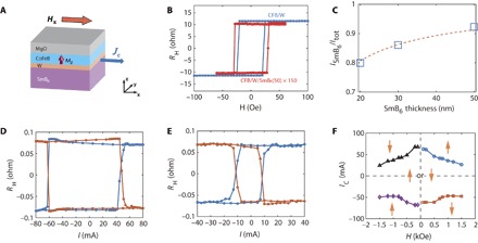
Fig. 3. SOT-induced switching of CFB/W/SmB6 devices.

(A) Schematic drawing of the device for SOT-induced switching experiment. (B) Hall resistance for the trilayer MgO(1.5)/CFB(1)/W(0.8) (blue) and MgO(1.5)/CFB(1)/W(0.8)/SmB6(50) (red). The latter is magnified 150 times. (C) Current distribution in SmB6 of CFB/W/SmB6 multilayers for various SmB6 film thicknesses. The red dashed line shows the calculation using longitudinal resistivity. SOT switching for CFB(1)/W(0.8)/SmB6(50) measured at 20 K (D) and 300 K (E), with external magnetic fields of 500 Oe (blue) and −500 Oe (red) applied along the x direction. (F) Switching phase diagram of CFB(1)/W(0.8)/SmB6(50) at 20 K.
