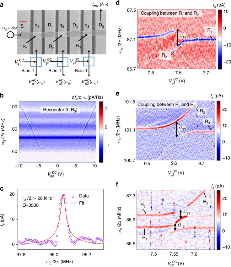
Fig. 1.
Sample structure and device characterization. a Scanning electron microscope photograph of a typical sample. An ~1-μm-wide graphene ribbon was suspended over four contacts, labeled as S, D1, D2, and D3, respectively. These contacts divide the ribbon into three sections, each with a gate of ~150 nm beneath the ribbon. A driving microwave with frequency ωd + δω is applied to contact S and is detected at contact D3 after mixing with another driving tone with frequency ωd applied to one or more of the control gates. Scale bar is 1 μm. b The differentiation of the mixed current dIx/dωd as a function of driving frequency ωd and gate voltage with V. Here, the frequencies of all resonators can be tuned from several tens of MHz to ~100 MHz by adjusting the dc gate voltages. c The mixing current as a function of the driving frequency ωd at voltage . Using a fitting process (see Supplementary Fig. 8), we extract the linewidth of the mechanical mode. The data were obtained at a driving power of −5 dBm. d, e Spectra of coupled modes R1 and R2 (d, where V and V) and R2 and R3 (e, where V and V). Strong couplings between these modes are manifested as avoided level crossings in the plots. Coupling strengths Ω12/2π ~ 240 kHz and Ω23/2π ~ 200 kHz are extracted from the plots. f The spectrum of R2 coupled to both R1 and R3. In this case, the gate voltages V and V are fixed

