Abstract
Objective
Foreign body response to indwelling cortical microelectrodes limits the reliability of neural stimulation and recording, particularly for extended chronic applications in behaving animals. The extent to which this response compromises the chronic stability of neural devices depends on many factors including the materials used in the electrode construction, the size, and geometry of the indwelling structure. Here, we report on the development of microelectrode arrays (MEAs) based on amorphous silicon carbide (a-SiC).
Approach
This technology utilizes a-SiC for its chronic stability and employs semiconductor manufacturing processes to create MEAs with small shank dimensions. The a-SiC films were deposited by plasma enhanced chemical vapor deposition and patterned by thin-film photolithographic techniques. To improve stimulation and recording capabilities with small contact areas, we investigated low impedance coatings on the electrode sites. The assembled devices were characterized in phosphate buffered saline for their electrochemical properties.
Main results
MEAs utilizing a-SiC as both the primary structural element and encapsulation were fabricated successfully. These a-SiC MEAs had 16 penetrating shanks. Each shank has a cross-sectional area less than 60 μm2 and electrode sites with a geometric surface area varying from 20–200 μm2. Electrode coatings of TiN and SIROF reduced 1 kHz electrode impedance to less than 100 kΩ from ~2.8 MΩ for 100 μm2 Au electrode sites and increased the charge injection capacities to values greater than 3 mC/cm2. Finally, we demonstrated functionality by recording neural activity from basal ganglia nucleus of Zebra Finches and motor cortex of rat.
Significance
The a-SiC MEAs provide a significant advancement in the development of microelectrodes that over the years has relied on silicon platforms for device manufacture. These flexible a-SiC MEAs have the potential for decreased tissue damage and reduced foreign body response. The technique is promising and has potential for clinical translation and large scale manufacturing.
INTRODUCTION
Chronically implanted microelectrode arrays (MEAs) for recording extracellular neural activity are central to scientific studies of neural circuit function[1–7]. These recordings help in understanding how neurons encode information and how neural signals can be decoded to provide insights into brain adaptation and learning. MEAs that penetrate the pial surface of the brain to provide cortical recordings are typically fabricated in silicon using thin-film processing techniques [3, 8, 9] or assembled as an array of polymer-insulated microwires [10, 11]. The cross-sectional dimension of the intra-parenchymal shanks or wires on these arrays vary with each particular design, but generally cross-sectional areas exceed 500 μm2 with a minimum transverse dimension greater than 10 μm. The most common MEAs of this type are those based on the University of Michigan design (Michigan Probes)[3, 9], and those developed at the University of Utah known as the Utah Array[12]. The ability of these multielectrode arrays to provide reliable chronic recordings is limited by the foreign body response and insertion trauma that results in gliosis, scar formation, and a substantial loss of viable neurons within about 50 μm of the electrode site[7, 13–16]. In addition, degradation of polymer encapsulation, loss of low impedance coatings at electrode sites, and delamination in thin-film multilayer structures have been identified as likely contributors to the reduced reliability of these devicesfor chronic recording[17, 18].
Recently, it has been recognized that the severity of the foreign body response is greatly reduced with implanted microelectrodes that have transverse cross-sectional dimension less than approximately 10 μm[13, 19–21]. Polymer insulated carbon fiber microelectrodes with shank diameters of 8.4 μm or less have demonstrated minimal gliosis and provided high quality single-unit recordings in acute and chronic studies[14, 16, 22–25]. However, it has proved challenging to manufacture carbon-fiber MEAs by processes that are amenable to fabricating large numbers of MEAs with a consistent electrode geometry. Here, we report on the development of MEAs based on amorphous silicon carbide (a-SiC). Amorphous SiC has emerged as a promising material for encapsulating implanted neural devices[26–29]. Films of a-SiC are well-tolerated in the cortex and resistant to corrosion or dissolution in saline[29–32]. In addition, a-SiC exhibits high intrinsic stiffness and, as a thin-film, is highly flexibility, comparable to carbon fiber microelectrodes.
The a-SiC MEAs fabricated for this study have intra-parenchymal shanks with a maximum transverse dimension of 10 μm and cross-sectional area less than about 60 μm2. These extremely small dimensions result in electrode sites with geometric surface areas (GSAs) less than 200 μm2 and potentially as small as 20 μm2. Consequently, the electrodes have a higher impedance and more limited charge-injection capacity for stimulation than typical silicon-based microelectrodes. However, the electrode sites are sufficiently small, in at least one dimension, to exhibit ultramicroelectrode (UME) behavior[33–35] and consequently higher charge densities, injectable charge per unit area, than larger microelectrodes with GSAs greater than 1000 μm2. The electrochemical behavior of both titanium nitride (TiN) and sputtered iridium oxide (SIROF) UMEs on the a-SiC MEAs has been investigated in buffered physiological saline with a notable decrease in impedance and increase in charge-injection capacity compared with microelectrodes (electrodes with typical GSA~2000 μm2) of the same electrode materials. Finally, the ability of a-SiC UMEs to provide neural recordings was evaluated acutely in the basal ganglia nucleus of the Zebra Finch and in the motor cortex of rat.
METHODS
The a-SiC MEAs were developed using standard thin-film fabrication processes. The a-SiC films were deposited by plasma enhanced chemical vapor deposition (PECVD) and patterned by thin-film photolithographic techniques. Electrode sites, bond pads and the device geometry were defined by reactive ion etching using an SF6 plasma chemistry. Electrical connection to the a-SiC MEAs was achieved by mounting an Omnetics connector directly on the array. The assembled devices were characterized inphosphate buffered saline ( PBS) for their electrochemical properties, and evaluated in the basal ganglia nucleus of Zebra Finches and in the motor cortex of rat for their neural recording capabilities.
PECVD a-SiC deposition
Amorphous SiC films were deposited in a PlasmaTherm Unaxis 790 Series PECVD system at a substrate temperature of 325°C, RF power density of 0.20 Wcm−2 (13.56 MHz), and pressure of 1000 mTorr using a reactive gas mixture of SiH4 and CH4 at flow rates of 12 sccm and 36 sccm respectively. The total gas flow rate into the reaction chamber was maintained at 800 sccm using Ar as the carrier gas. Scanning electron microscopy (SEM) and atomic force microscopy (AFM) were used to determine the surface morphology of the films. Film thickness was measured with a Nanometric NanoSpec 6100 analyzer using data collected from 20 randomly selected points across the a-SiC film. Film stress was measured using silicon control wafers with a Toho Technology FLX-2320 stress analyzer and estimated using the Stoney equation[36].
Fabrication of a-SiC MEAs
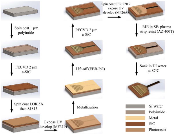
The multilayered a-SiC MEAs were fabricated on prime-grade 100 mm Si (100) wafers using polyimide (HD Microsystems, PI 2610) as a release layer between the a-SiC MEA and silicon substrate. The detailed fabrication steps are summarized in Figure 1. Briefly, an approximately 1 μm polyimide film is spin-coated onto the Si wafer and cured at 350°C for one hourunder nitrogen. A 2 -μm thick a-SiC film is then deposited over the polyimide. Metal traces are formed on the a-SiC by sputter deposition using lift-off photolithography to define the metal pattern. To facilitate liftoff, a non-photosensitive LOR 5A (Microchem Inc) layer and a photosensitive Shipley (S1813, Microposit) photoresist layer are spin-coated consecutively on the a-SiC in a process designed to create an undercut in the two-layer resist. The metallization is deposited by DC sputtering and comprised either a three-layer coating of Ti/Au/Ti (30 nm/250 nm/30 nm, thickness) or a four-layer coating of Ti/Au/Pt/Ti (30 nm/150 nm/150 nm/30 nm, thickness). After the metal deposition, the carrier wafers are immersed in EBR-PG (Microchem Inc.) for metal lift-off. A second 2-μm layer of a-SiC is deposited over the metal traces to provide complete encapsulation of the metal in a-SiC. Vias for the electrode sites and bond pads are opened by removing the top a-SiC layer and upper titanium layer by reactive ion etching in an SF6 plasma at low pressure using an inductively coupled plasma (ICP) etcher (PlasmaTherm). The opening for the electrode sites was 2 μm by 50 μm, resulting in a site GSA of 100 μm2 in the absence of a low impedance electrode coating. Singulation of the a-SiC into individual MEAs is also accomplished in a second SF6 RIE step in which the a-SiC superstructure of the MEA is protected by a 6.5 μm thick layer of photoresist. After the RIE singulation process, the devices are soaked in AZ400T (AZ Electronic Materials) at 70°C to remove the remaining photoresist and then thoroughly rinsed in deionized water to remove remaining residue. In the final step, the wafers with a-SiC MEAs are immersed in deionized water at 87°C until the arrays release from the silicon wafer. Electrical connection to the a-SiC MEAs is obtained with an Omnetics connector mounted on the array using a solder reflow process and indium-based solder paste (Indium Corporation). A medical grade epoxy (Loctite) or dental acrylic (Flow-It ALC, Pentron) is then cured around the base of the Omnetics connector to provide mechanical strength.
Figure 1.
Microfabrication of amorphous silicon carbide microelectrode arrays (a-SiC MEAs). The process flow features at least three photolithography steps: one for defining the metal traces and electrodes, a second for patterning the top a-SiC layer for electrode site and bond pad openings, and a third photolithography step to singulate the a-SiC device geometries. A fourth lift-off lithography step is used (not shown) to restrict deposition of SIROF or porous TiN low impedance coatings to the electrode sites.
Low impedance electrode coatings
Low impedance coatings of sputtered iridium oxide (SIROF) or porous titanium nitride (TiN) were deposited onto electrode sites by reactive DC sputtering from iridium or titanium metal targets, respectively. Lift-off photolithography was used to restrict deposition to the electrode sites. However, a narrow band of the electrode coatings is deposited on the rim of the a-SiC at the electrode site resulting in electrode coatings with approximately a 150 μm2 (3 μm × 50 μm) GSA. The film thickness, determined by surface profilometry, was 300 nm for the SIROF coatings and 2 μm for the TiN coatings.
Electrochemical characterization
The electrochemical properties of the a-SiC UMEs were evaluated at room-temperature in inorganic phosphate buffered saline (PBS), having a composition of 126 mM NaCl, 22 mM NaH2PO4.7H2O and 81 mM Na2HPO4.H2O at a pH of 7.2, that was purged with argon to remove dissolved oxygen gas[37, 38]. The electrochemical characterization included cyclic voltammetry (CV), electrochemical impedance spectroscopy (EIS) and voltage transient measurements in response to constant current pulsing. The cathodal charge storage capacity (CSCc) of the electrodes was calculated from the CV measurements that were made at a sweep rate of 50 mV/s between potential limits of −0.6 V and 0.8 V versus Ag|AgCl[39]. A three-electrode cell comprising the SIROF or Pt UME working electrode, a large surface area Pt counter electrode and a Ag|AgCl reference electrode was used for all measurements. EIS measurements were made with a 10 mV rms AC perturbation about the open circuit potential over a 1 Hz to 105 Hz frequency range. The CV and EIS data were acquired with a Gamry Reference 600plus potentiostat using vendor-supplied software. The stimulation charge-injection capacity of the electrodes was determined from voltage transient measurements using cathodal monophasic current pulsing combined with active control of the interpulse potential of the electrode to maintain charge-balance [40]. Anodic bias potentials of 0.0 V to 0.8 V versus Ag|AgCl in the interpulse period were investigated [39]. A pulse width of 200 μs and repetition rate of 50 pulses per second were used throughout the study. The maximum charge-injection capacity of the electrode coatings was determined by increasing the current during pulsing until the iR-corrected electrochemical potential of theelectrode reached a value of −0.6 V Ag|AgCl.
Acute implantation and neural recording
In the first study of neural recording with a-SiC MEAs, the arrays were implanted in the basal ganglia nucleus, area X, of Zebra Finch. All procedures were approved by the Institutional Animal Care and Use Committee of Boston University and follow methods previously described[22]. Briefly, the zebra finches were anesthetized with 4 % isoflurane (mixed with pure oxygen at 0.5 L/min flow rate) and maintained at 1–2 % isoflurane during the surgical procedure. A 120 μL dose of analgesic Meloxican (1 % in PBS) was injected intramuscularly into the right breast at the start of the surgical procedure and the animal was placed into a stereotaxic instrument. An incision was made in the scalp anterior-posterior (AP) axis and the outer bone leaflet removed using a dental drill. Using an ophthalmic scalpel, the lower bone leaflet was carefully removed[41] exposing a 1 mm diameter portion of the dura. An incision of 1 mm was performed in the dura to facilitate the MEA penetration into the brain. The a-SiC MEAs were mounted on a manual manipulator attached to the stereotaxic instrument and slowly lowered through the brain. Prior to mounting the arrays, the a-SiC MEAs were embedded in a droplet of polyethylene glycol (PEG) following methods described elsewhere[23]. Recordings were made from spontaneously active cells using an Intan RHD 2000 system with a 16-channel unipolar input head stage. Data was sampled at 20 kHz with filter cutoffs set to 350 Hz and 7.5 kHz.
Neural recording with the a-SiC MEAs was also investigated acutely in rat motor cortex using the procedure described below and approved by the institutional animal care and use committee (IACUC) at the University of Texas at Dallas. The MEAs were implanted in the motor cortex of male Long-Evans (Charles River Labs, MA) rats (~300 gram) under anesthetized conditions. The animals were anesthetized by intraperitoneal injection of a mixture of 65mg Ketamine, 13.33mg Xylazine and 1.5mg Acepromazine per kg body weight of the animal post isoflurane (2–3%) induction. Atrophine (0.05mg/kg) was also administered to prevent cardiovascular depression under anesthesia. The hair of the animals’ scalp was expunged, cleaned and disinfected with 10% povidone iodine solution and 70% ethanol. The head of the animal was then placed in a stereotaxic frame. Prior to the midline incision, dexamethasone was administered subcutaneously over the shoulders followed by 0.16 cc of 0.5% lidocaine under the incision site. The skull was exposed by retracting the surrounding skin and muscles and scraping the periosteum above the planned implant site. A dental drill (Fine Science Tools, Foster City, CA) was used to create holes on the contralateral side of the skull to secure two bone screws for grounding and securing of the Omnetics connector. A 2mm by 2mm craniotomy was performed anterior to the bregma for array implantation. To prevent thermal damage due to drilling, the skull surface was periodically flushed with sterile saline at 37°C. To constrict local blood vessels and reduce bleeding, gauze moistened with epinephrine at 1 mg/ml was applied to the craniotomy for 1 minute, followed by an additional flush of the craniotomy with 0.9% saline. The dura (~80–100μm) was gently retracted with a 30 gauge needle tip. The a-SiC MEAs were mounted onto a custom built array holder and aligned to the skull opening with the electrode tips facing the cortex using a micro-positioner (Kopf Instruments, CA) attached to the stereotaxic frame. The PEG stabilized tips were advanced using the micro-positioner set at a speed of 50 μm/s to ensure dissolution of the PEG as the arrays are advanced into the brain. The arrays were inserted to a depth of ~2–3 mm from the cortical surface. Spontaneous neural activity was recorded using a 32 channel OmniPlex data acquisition system (Plexon Inc., USA). Post signal amplification (20 X), the signal band passed filtered between 50 Hz and 8 kHz was digitized at 40 kHz and recorded for 5 minutes.
RESULTS
Residual film stress of the a-SiC
A significant challenge in developing the a-SiC MEAs was control of the intrinsic film stress. Building multilayer structures requires stress balance between individual layers to avoid interlayer delamination, and to maintain the desired planar geometry once the MEAs are removed from the silicon carrier wafer. For PECVD a-SiC, the intrinsic film stress is dependent on deposition conditions such as RF power density, deposition temperature, deposition pressure and the flow rates of the SiH4 and CH4 reactive gases[42–45]. Using the deposition conditions described above, we obtained amorphous films with a compressive stress in the range of 80–120 MPa for a 2 μm thick film. To balance the stress across the multilayer device, the thickness and tensile stress in the Ti/Au/Ti or Ti/Au/Pt/Ti metallization was adjusted by controlling sputtering power and pressure during metal deposition. A metal stress of 40–100 MPa in tension produced planar MEAs with good interlayer adhesion.
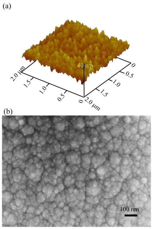
As shown in Fig. 2(a), the rmssurface roughness for the 2 μm thick a-SiC was 3.75 nm, indicating a surface that is sufficiently smooth for subsequent photolithographic processing. SEM inspection of the 2 μm thick a-SiC films under high magnification revealed a nodular surface morphology as shown in figure 2(b).
Figure 2.
Surface morphology and topography of a-SiC films. (a) AFM image (2μm × 2μm) and (b) SEM images show the surface morphology of 2 μm thick PECVD amorphous-SiC deposited on a silicon wafer. The surface roughness estimate from the AFM is below 4 nm rms.
Amorphous-SiC MEA fabrication
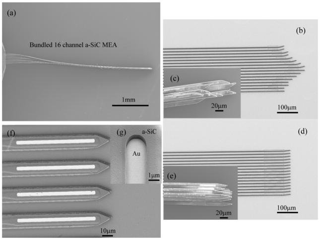
For intracortical studies, the a-SiC MEAs were fabricated with 16 penetrating shanks with one electrode per shank. Each shank was 4 – 5 μm thick, 9 μm wide and terminated in a sharply pointed tip with an angle of 10 –14. The shank length for this study was 4 mm and the GSA of the Pt and Au electrode sites was 100 μm2 and 150 μm2 (3 μm × 50 μm) for the SIROF or TiN coated electrodes. The electrode sites were located at the distal end of the shank as shown in Fig. 3. The metal interconnects, either gold or a gold/platinum bilayer, run approximately along the neutral axis of each shank, connecting the electrode sites at the distal end and bond pads at the proximal end. A top layer a-SiC was deposited over the metallization and the first layer of a-SiC to completely encapsulate the metal traces.
Figure 3.
SEM images show released bundles of a-SiC MEAs (a, c, and e) taken at 5kV, and shanks still attached to the carrier silicon wafer (b, d, f, and g) taken at 2kV acceleration voltage. (a) The shanks of a released a-SiC MEA form a bundle when drawn out of water. The tip of the bundle is shaped by the layout design of the shank arrays, as shown in (b–c and d–e), (f) shows the exposed electrode tip at the distal end of the shank and (g) shows the side wall profile of the exposed electrode site at a 25 degree viewing angle.
Openings in the top a-SiC were formed by reactive ion etching to expose the electrode sites and bond pads. Figures 3(f) and 3(g) show an electrode site opened through the top a-SiC layer. The photolithographic patterning process ensures control of the GSA of the electrode site which is recessed approximately 2 μm. As seen in Fig. 3(g), the ICP etching process produces a near-vertical side wall profile. The depth of the recess is such that the current distribution during stimulation should be approximately uniform over the surface of the recessed electrode[46, 47].
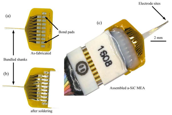
In order to release the devices from the carrier wafer, the a-SiC MEAs are immersed in DI water. When carefully withdrawn from the DI water, the 16 individual shanks form a shank bundle with an approximate diameter of 40 μm (Fig. 3(a)). The tip of the bundle is shaped by the layout design of the shank arrays. Fig. 3(b) and 3(d) shows two different tip configurations of as fabricated devices prior to release and their resultant bundle-profiles (Fig. (3(c) and 3(e)) after release. Bonding pads, 750 × 500 μm in dimension, with a 635 μm pitch designed to mate with a 16 channel Omnetics connector (Omnetics, A79040-001), are located at the proximal end of the array. An indium-tin eutectic solder paste (Indium Corporation) reflowed at 200 °C was used in creating electrical connection between the bond pads and the connector. Fig. 4 shows the a-SiC MEA after fabrication (4(a)), after the Omnetics connecter has been soldered (4(b)) and after the connector is securely fixed with epoxy ( 4(c)).
Figure 4.
Optical micrographs show that the 16 shanks naturally bundle when the as-fabricated device is pulled out of the deionized water. Omnetics connectors were mounted on the arrays using a solder reflow process and medical grade epoxy. The figure shows (a) the as-fabricated a-SiC MEA after release from deionized water, (b) after an Omnetics connector is soldered onto the bond pads and (c) a packaged device for implantation or in vitro electrochemical characterization.
Electrochemical characterization
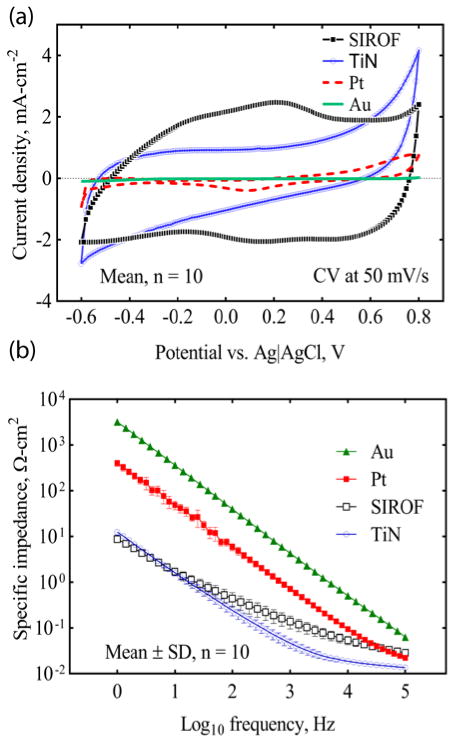
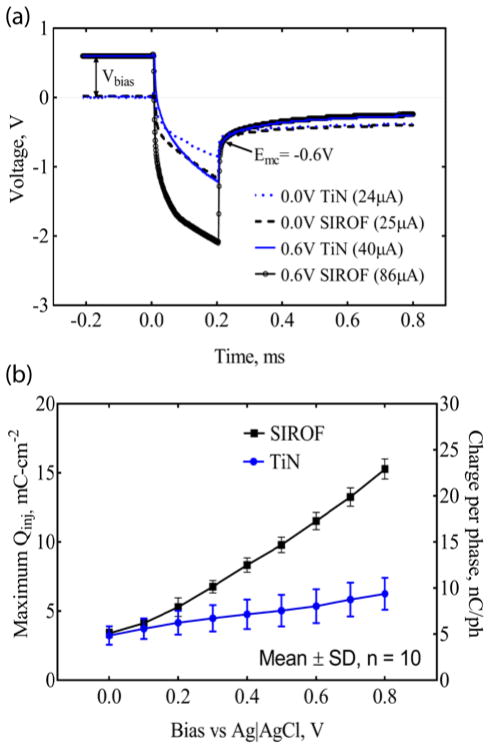
Cyclic voltammograms (CVs) of gold, platinum, SIROF and porous TiN UMEs on the a-SiC MEAs are compared in Fig. 5(a). Each CV is an average of 10 CVs from one MEA. The CSCc of the SIROF and TiN-coated UMEs was 35±2.2 mC/cm2 and 12±2.8 mC/cm2 (Mean±SD, n=10), respectively. The uncoated platinum and gold UMEs had lower CSCc’s of 10±1.7 mC/cm2 and 2±0.3 mC/cm2, respectively. These CSCc’s were calculated over a nominal water window range of −0.6 V to 0.8 V Ag|AgCl and a higher CSCc would be expected for the TiN if the negative potential limit was extended to the TiN water reduction potential which is close to −0.9 V Ag|AgCl[39, 48]. Impedance spectra for each UME, normalized to the electrode GSA, are compared in Fig. 5(b). As expected, the UME impedance measured at 1 kHz was reduced by at least two orders of magnitude for both TiN and SIROF coatings compared to the gold UMEs. The average impedance values measured at 1 kHz for SIROF, TiN and Pt are 90.2±26.1 kΩ, 31.1±7.3 kΩ and 481.3±67.9 kΩ respectively, compared to 2.86±0.3 MΩ for Au UME sites. The ability of the SIROF and TiN-coated UMEs to deliver charge for stimulation was investigated by voltage transient measurements in response to constant current pulsing. Fig. 6(a) shows representative voltage transient responses for anodically biased and unbiased electrodes at the current amplitude that drives the iR-corrected electrode potential (Emc) to the −0.6 V water electrolysis limit[39, 48, 49]. The average maximum driving current for TiN-coated UMEs was 24.2 μA (0 V bias) and 46.9 μA (0.8 V bias), and for SIROF-coated UMEs, 25.4 μA (0 V bias) and 114.6 μA (0.8 V bias). The maximum charge injection capacity (Qinj) of the TiN and SIROF UMEs as a function of anodic bias is shown in figure 6(b).
Figure 5.
Electrochemical properties of a-SiC UMEs coated with SIROF, TiN and Pt compared with Au. (a) Cyclic voltammogram measured at 50mV/s between −0.6V and 0.8V limits. (b) Electrochemical impedance spectroscopy measured using a 10 mV rms AC sinusoid.
Figure 6.
Electrical stimulation capabilities of ultramicroelectrodes (a) Voltage transient response to current waveforms for TiN and SIROF electrodes biased at 0.6V vs Ag|AgCl (solid lines) and without anodic bias (dash lines). The electrodes were polarized to a cathodal potential limit of −0.6 V. The average current passed across the interface within the ‘safe’ electrochemical limit is 86.4 μA for SIROF (0.6 V bias) and 40.2 μA for TiN (0.6 V bias). (b) Maximum charge injection capacity and charge per phase as a function of interpulse bias. (Frequency= 50 pps, Pulse width = 200 μs).
The charge injection capacity for SIROF increased with anodic bias from ~ 3.4 mC/cm2 at a 0.0 V bias to 15.3 mC/cm2 at a 0.8 V bias. A similar trend was observed for TiN whose charge injection capacity increased monotonically from 3.2 mC/cm2 to 6.2 mC/cm2 over the same anodic bias range. The Qinj values reported here are generally higher than those reported for microelectrode arrays (electrode GSAs ~ 2000 μm2) with the same electrode coatings[39, 48].
Neural recording
To evaluate the functionality of the a-SiC MEAs, the arrays were implanted in Zebra Finch basal ganglia nucleus Area X. Following the method introduced previously[23], the shanks of a-SiC MEAs were coated with poly-ethylene glycol (PEG).
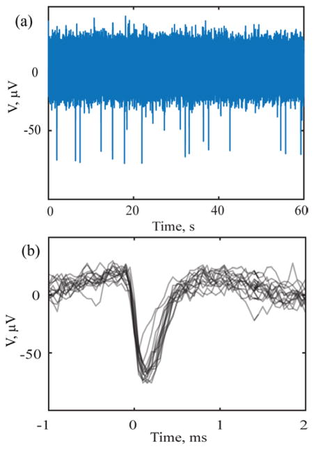
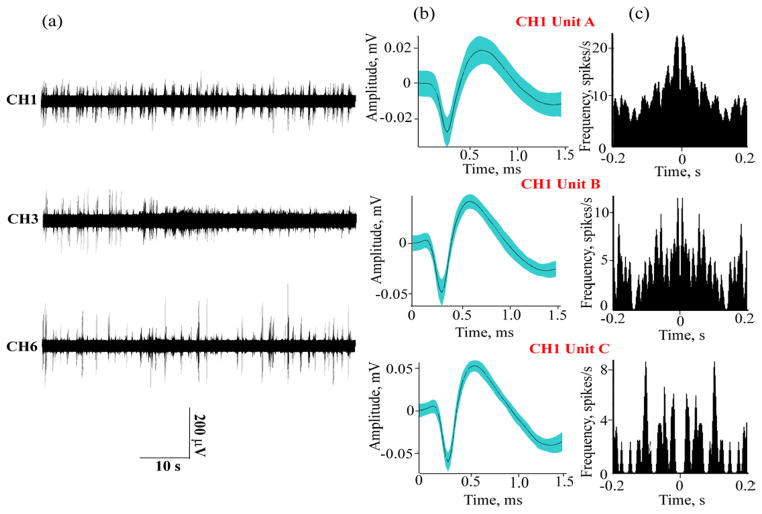
PEG-coatings proved reliable in creating stiff assemblies in which individual shanks are held apart prior to implanting. During insertion, the PEG dissolved from the comb allowing the shafts to enter the tissue without buckling. We determined an insertion speed of 50 μm/s to be adequate to ensure dissolution of the PEG during implantation. It is however possible that some PEG may remain on the penetrating shanks and the effect of the PEG-residue on the chronic functionality of the devices is yet to be evaluated. The data shown in Fig. 7 were recorded in an acute preparation immediately after surgery using a Pt a-SiC UME with 100 μm2 GSA. Fig. 7(a) shows the recorded voltage trace and 7 (b) is an overlay of neuronal spike waveforms from a single channel demonstrating single unit spiking activity. The feasibility of recording spontaneous activity with PEG-stabilized a-SiC MEAs arrays was also tested in anesthetized rat motor cortex. For this study, a 16 shank a-SiC MEA with SIROF-coated UMEs was mounted on a motorized drive and inserted into the cortex. Figure 8(a) shows spontaneous neural activity recorded simultaneously on three channels in a single trial. Distinct spiking activity across multiple channels confirms that the electrode array recorded from spatially selective neuronal population. Post-processing of the recorded activity revealed depth dependent single unit activity on 9 of the 16 electrodes, as the electrodes were inserted incrementally to 2–3 mm below the cortical surface. Array yield, quantified as number of electrodes with identified single unit spikes was 56% for the acute trial
Figure 7.
Acute neural recording immediately following implantation in basal ganglia of Zebra Finch brain. The 16 recorded channels showed no strong coupling between contacts (a) single channel acute voltage trace with a subcutaneous reference on the head and (b) an overlay of a neuronal spike waveforms, detected by setting the threshold of the trace in (a) at − 50 μV.
Figure 8.
Spontaneous neural activity in rat motor cortex: (a) simultaneous spike activity recorded across three channels using the a-SiC MEA; (b) sorted single units on CH1 with average peak-to-peak amplitudes of 45 μV (Unit A), 87 μV (Unit B) and 114 μV (Unit C); and (c) the corresponding autocorrelograms processed with a bin size of 2 ms.
The single unit mean peak-to-peak amplitudes across all recorded electrodes were in the 45–200 μV range. Fig 8(b) shows 3 single unit signals from Channel 1 (CH1) identified after offline processing of the neural spikes. The waveforms of the units show a mean peak to peak amplitudes of 45 μV, 87 μV and 114 μV for Unit A, Unit B and Unit C respectively. The spike shapes shown here are typical to previously reported cortical single unit recording [50–52]. Fig. 8(c) shows the corresponding autocorrelograms of the sorted units in 8(b) computed with a bin size of 2 ms and smoothing with a Gaussian filter (filter width = 3 bins). The autocorrelation function show a bimodal distribution which clearly indicate distinct single unit spikes. While Units B and C have a stronger bimodal distribution with refractory periods >1ms, Unit A has a weaker distribution with some multi-unit contamination in the sorted units, indicated from the firing frequency distribution.
DISCUSSION
Minimizing insertion trauma and the foreign body response to implanted multielectrode arrays is an important objective in the development of recording and stimulation devices for brain-machine interfaces in both research and clinical settings. The insertion trauma and foreign body response lead to electrode encapsulation and death or damage of neurons at distances up to approximately 100 μm from the implant site[6, 7, 53–55]. The length scale of this tissue reaction is detrimental to neural recordings, since action potential amplitudes decay exponentially with distance from an electrode[56–58]. As a result, chronically implanted electrodes are typically limited to recording from a larger population of weak signals, limiting spike sorting and single neuron resolution - a problem that is particularly severe for small animal models with small, densely packed neurons. Approaches to minimizing the foreign body response have included the development of polymer-based electrodes that reduce the elastic modulus mismatch between the electrode and neural tissue[59–63], the development of wireless interfaces that eliminate wired connections and reduce electrode micromotion[64–66], and the use of stiff but highly flexible electrodes with cross-sectional dimensions typically smaller than 10 μm[16, 22, 23, 25]. The a-SiC MEAs, described here, are designed to address insertion trauma and foreign body response by employing the latter strategy with the maximum transverse dimension of individual shanks under 10 μm and the cross-sectional area of individual shanks under 60 μm2. One obvious benefit of employing a-SiC as the primary material of array construction is the ability to fabricate devices by established thin-film deposition and photolithographic patterning processes. The thin-film fabrication of a-SiC MEAs is highly reproducible with inherent flexibility in the design of the arrays.
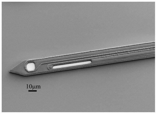
It is possible to fabricate arrays with individual shanks having multiple electrode sites along the length of the shanks and optionally with different shapes and GSAs. An example of a two-electrode combination of gold electrodes with a GSA of 100 μm2 in a 2 × 50 μm and 10 × 10 μm configuration at the distal end of a shank is shown in Fig. 9.
Figure 9.
A SEM image of the distal tip of an a-SiC UME shank with two electrode sites located on the same shank. The GSA of the exposed Au electrode sites is 100 μm2 but with unequal perimeter. The perimeter of the square electrode site is 40 μm versus 104 μm for the rectangular site.
This UME geometry is part of an ongoing study to investigate the effect of perimeter-to-area ratio on the in vivo and in vitro electrochemical properties of ultramicroelectrodes. Although arrays with individual shanks having a tetrode layout have been fabricated, we have yet to evaluate the possibility of using this configuration for spike sorting.
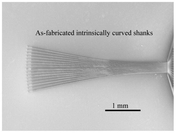
Similarly, it is possible to build in geometries that promote splaying when using the bundling properties of the shanks to insert the MEAs into tissue. A 16-channel MEA with shanks having intrinsic curvature intended to direct the splaying action during insertion is shown in Fig. 10. An array with the splayed geometry forms a monolithic and tight bundle of shanks when withdrawn from water so that insertion into tissue can be initiated without the shanks buckling.
Figure 10.
A SEM image of a-SiC MEA with a built-in shank curvature. The intrinsic curvature is expected to improve splaying capabilities of the a-SiC MEAs which form bundles when drawn out of water.
While we observed the bundled shanks penetrate into cortex in the absence of PEG coatings, we have yet to demonstrate that the intrinsic curvature promotes splaying while minimizing insertion trauma. Nonetheless, the geometries shown in Figs. 9 and 10 give some indication of the options available in designing UME arrays to address different study needs.
Irrespective of these benefits, a consequence of reducing the shank cross-sectional dimensions is that at least one linear dimension of the electrode site is in the ultramicroelectrode range[33–35] and the reduced GSA results in an electrode impedance that is higher than that of a typical microelectrode used for neural recording[67].
However, UME-dimensioned electrodes have provided high quality neural recordings in both acute and chronic preparations[16, 22, 23]. In previous studies, Gardner and colleagues developed methods of assembling carbon fiber UME arrays and evaluated these electrodes in chronic songbird preparations[22].
These studies confirmed that UMEs can provide stable long-term chronic neural recordings in behaving animals and that small shank dimensions result in minimal foreign body response. Similar studies also produced important findings regarding the nature of song stability at the level of neural coding in the high vocal center (HVC) of Zebra Finchpre -motor cortex[68, 69].
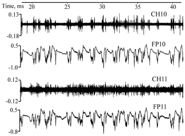
Implanted a-SiC MEAs successfully recorded simultaneous neural activity in the two animal models evaluated. Since the in vivo studies were intended for pilot feasibility evaluation, the analysis of the recorded signals was limited to the observations of single unit spikes from spontaneous neural activity. Figure 11 shows the raw traces for both spike activity obtained from high-pass filtered data and the corresponding local field potentials (low-pass filtered data at <350Hz) showing the correlations in the temporal distribution similar to those reported elsewhere[70, 71]. Detailed analysis of the local field potentials, especially in different low frequency bands like delta, spindle and gamma among others will be evaluated in future studies.
Figure 11.
Raw traces showing simultaneously recorded spontaneous spike activity on channel 10 and 11 (CH10 and CH11) and their corresponding local field potentials (FP10 and FP11). (spike and local field potential amplitudes in mV).
Electrical stimulation of neural activity is more challenging with UMEs. The use of SIROF or TiN partially mitigates the impact of reduced electrode size. Charge-injection capacities of 11.5 mC/cm2 and 5.4 mC/cm2, respectively, were observed for 200 μs pulses in buffered saline when the UMEs are biased to 0.6 V, and as high as 15.3 mC/cm2 and 6.3 mC/cm2 respectively at 0.8 V bias. These charge-injection capacities are notably larger than those obtained with similar coatings on larger microelectrodes[39, 48, 72, 73]. For example, using similar pulse parameters, charge injection limits of approximately 4 mC/cm2 and 0.87 mC/cm2 were estimated for 4000 μm2 iridium oxide and TiN microelectrodes respectively[48]. While the small size of UMEs results in an increase in charge-injection capacity the total deliverable charge remains low even with electrode coatings. The maximum charge that could be delivered in a 200 μs pulse was 23 nC/ph for SIROF and 9 nC/ph for TiN UMEs. The uncoated Pt and Au UMEs exhibited charge per phase values less than 1 nC/ph, likely below the microelectrode charge threshold for neural activation[74]. It remains to be seen whether reduced tissue damage and the likely presence of healthy neurons in much closer proximity to UME sites compared with conventional microelectrodes will result in reduced charge thresholds for neural activation. The UME concept originated in the context of chemical sensing and quantification using voltammetric electrodes and the extension of this concept to stimulation electrodes has limitations[75]. A UME may be broadly defined as an electrode in which transport of the electrolyzed species to the electrode occurs via spherical or hemispherical diffusion[33, 76]. Geometrically, at least one dimension of a UME must be less than the diffusion layer thickness of the species involved in the electrode reactions[33]. For neural stimulation electrodes the electroactive species are the counterions that preserve electrode neutrality and these species are charged.
CONCLUSIONS
MEAs have been fabricated using a-SiC as the primary material of construction. The arrays are designed with shanks that penetrate into target neural tissue with cross-sectional dimensions that are expected to minimize insertion trauma and reduce foreign body response. By employing conventional thin-film processing techniques, a wide variety of array geometries are possible including the placement of multiple electrodes on a single shank. Since the cross-sectional dimensions of the shanks are typically 5 μm by 10 μm or less, the electrode sites have ultramicroelectrode dimensions with geometric surface areas between 20 μm2 and 200 μm2. These electrodes recorded spontaneous neural activity in acute Zebra Finch nucleus and rat cortical preparations. Implantation into cortex using bundled a-SiC shanks was also demonstrated. Low-impedance coatings of SIROF and porous TiN deposited on the UME sites were investigated as a means of providing sufficient charge for neural stimulation. These coatings provided more than 1 nC/ph within water electrolysis limits in a 200 μs pulse, which is comparable to neural activation thresholds reported in some microelectrode studies[74]. However, additional studies are needed to determine the extent to which the a-SiC MEAs minimize foreign body response and whether the UMEs can provided functionally useful levels of charge-injection for stimulation.
Acknowledgments
This work was funded by the National Institute of Health under Grant No. U01NS090454 awarded to Boston University (Timothy Gardner, PI).
Footnotes
Conflict of interest: none declared Abstract
References
- 1.Rousche PJ, Normann RA. Chronic recording capability of the utah intracortical electrode array in cat sensory cortex. J Neurosci Methods. 1998;82:1–15. doi: 10.1016/s0165-0270(98)00031-4. [DOI] [PubMed] [Google Scholar]
- 2.Suner S, Fellows MR, Vargas-Irwin C, Nakata GK, Donoghue JP. Reliability of signals from a chronically implanted, silicon-based electrode array in non-human primate primary motor cortex. IEEE Trans Neural Syst Rehabil Eng. 2005;13:524–541. doi: 10.1109/TNSRE.2005.857687. [DOI] [PubMed] [Google Scholar]
- 3.Vetter RJ, Williams JC, Hetke JF, Nunamaker EA, Kipke DR. Chronic neural recording using silicon-substrate microelectrode arrays implanted in cerebral cortex. IEEE Trans Biomed Eng. 2004;51:896–904. doi: 10.1109/TBME.2004.826680. [DOI] [PubMed] [Google Scholar]
- 4.Williams JC, Rennaker RL, Kipke DR. Long-term neural recording characteristics of wire microelectrode arrays implanted in cerebral cortex. Brain Res Protoc. 1999;4:303–313. doi: 10.1016/s1385-299x(99)00034-3. [DOI] [PubMed] [Google Scholar]
- 5.Ludwig KA, Uram JD, Yang J, Martin DC, Kipke DR. Chronic neural recordings using silicon microelectrode arrays electrochemically deposited with a poly(3,4-ethylenedioxythiophene) (PEDOT) film. J Neural Eng. 2006;3:59–70. doi: 10.1088/1741-2560/3/1/007. [DOI] [PubMed] [Google Scholar]
- 6.Polikov VS, Tresco PA, Reichert WM. Response of brain tissue to chronically implanted neural electrodes. J Neurosci Methods. 2005;148:1–18. doi: 10.1016/j.jneumeth.2005.08.015. [DOI] [PubMed] [Google Scholar]
- 7.Biran R, Martin DC, Tresco PA. Neuronal cell loss accompanies the brain tissue response to chronically implanted silicon microelectrode arrays. Exp Neurol. 2005;195:115–126. doi: 10.1016/j.expneurol.2005.04.020. [DOI] [PubMed] [Google Scholar]
- 8.Wise KD, Angell JB, Starr A. An Integrated-Circuit Approach to Extracellular Microelectrodes. IEEE Trans Biomed Eng. 1970;BME-17:238–247. doi: 10.1109/tbme.1970.4502738. [DOI] [PubMed] [Google Scholar]
- 9.Kipke DR, Vetter RJ, Williams JC, Hetke JF. Silicon-substrate intracortical microelectrode arrays for long-term recording of neuronal spike activity in cerebral cortex. IEEE Trans Neural Syst Rehabil Eng. 2003;11:151–155. doi: 10.1109/TNSRE.2003.814443. [DOI] [PubMed] [Google Scholar]
- 10.Nicolelis MAL, Dimitrov D, Carmena JM, Crist R, Lehew G, Kralik JD, Wise SP. Chronic, multisite, multielectrode recordings in macaque monkeys. Proc Natl Acad Sci. 2003;100:11041–11046. doi: 10.1073/pnas.1934665100. [DOI] [PMC free article] [PubMed] [Google Scholar]
- 11.Etemadi L, Mohammed M, Thorbergsson PT, Ekstrand J, Friberg A, Granmo M, Pettersson LME, Schouenborg J. Embedded ultrathin cluster electrodes for long-term recordings in deep brain centers. PLoS One. 2016;11:1–18. doi: 10.1371/journal.pone.0155109. [DOI] [PMC free article] [PubMed] [Google Scholar]
- 12.Nordhausen CT, Maynard EM, Normann RA. Single unit recording capabilities of a 100 microelectrode array. Brain Res. 1996;726:129–140. [PubMed] [Google Scholar]
- 13.Skousen JL, Merriam SME, Srivannavit O, Perlin G, Wise KD, Tresco PA. Reducing surface area while maintaining implant penetrating profile lowers the brain foreign body response to chronically implanted planar silicon microelectrode arrays. Progress in Brain Research. :167–180. doi: 10.1016/B978-0-444-53815-4.00009-1. [DOI] [PubMed] [Google Scholar]
- 14.Kozai TDY, Jaquins-Gerstl AS, Vazquez AL, Michael AC, Cui XT. Brain tissue responses to neural implants impact signal sensitivity and intervention strategies. ACS Chem Neurosci. 2015;6:48–67. doi: 10.1021/cn500256e. [DOI] [PMC free article] [PubMed] [Google Scholar]
- 15.Szarowski DH, Andersen MD, Retterer S, Spence AJ, Isaacson M, Craighead HG, Turner JN, Shain W. Brain responses to micro-machined silicon devices. Brain Res. 2003;983:23–35. doi: 10.1016/s0006-8993(03)03023-3. [DOI] [PubMed] [Google Scholar]
- 16.Yoshida Kozai TD, Langhals NB, Patel PR, Deng X, Zhang H, Smith KL, Lahann J, Kotov Na, Kipke DR. Ultrasmall implantable composite microelectrodes with bioactive surfaces for chronic neural interfaces. Nat Mater. 2012;11:1065–1073. doi: 10.1038/nmat3468. [DOI] [PMC free article] [PubMed] [Google Scholar]
- 17.Kane SR, Cogan SF, Ehrlich J, Plante TD, McCreery DB, Troyk PR. Electrical performance of penetrating microelectrodes chronically implanted in cat cortex. IEEE Trans Biomed Eng. 2013;60:2153–2160. doi: 10.1109/TBME.2013.2248152. [DOI] [PMC free article] [PubMed] [Google Scholar]
- 18.Barrese JC, Aceros J, Donoghue JP. Scanning electron microscopy of chronically implanted intracortical microelectrode arrays in non-human primates. J Neural Eng. 2016;13:26003. doi: 10.1088/1741-2560/13/2/026003. [DOI] [PMC free article] [PubMed] [Google Scholar]
- 19.Seymour JP, Kipke DR. Neural probe design for reduced tissue encapsulation in CNS. Biomaterials. 2007;28:3594–3607. doi: 10.1016/j.biomaterials.2007.03.024. [DOI] [PubMed] [Google Scholar]
- 20.Sanders JE, Stiles CE, Hayes CL. Tissue response to single-polymer fibers of varying diameters: Evaluation of fibrous encapsulation and macrophage density. J Biomed Mater Res. 2000;52:231–237. doi: 10.1002/1097-4636(200010)52:1<231::aid-jbm29>3.0.co;2-e. [DOI] [PubMed] [Google Scholar]
- 21.Stice P, Gilletti A, Panitch A, Muthuswamy J. Thin microelectrodes reduce GFAP expression in the implant site in rodent somatosensory cortex. J Neural Eng. 2007;4:42–53. doi: 10.1088/1741-2560/4/2/005. [DOI] [PubMed] [Google Scholar]
- 22.Guitchounts G, Markowitz JE, Liberti WA, Gardner TJ. A carbon-fiber electrode array for long-term neural recording. J Neural Eng. 2013;10:46016. doi: 10.1088/1741-2560/10/4/046016. [DOI] [PMC free article] [PubMed] [Google Scholar]
- 23.Patel PR, Na K, Zhang H, Kozai TDY, Kotov NA, Yoon E, Chestek CA. Insertion of linear 8. 4 μm diameter 16 channel carbon fiber electrode arrays for single unit recordings. J Neural Eng. 2015;12:46009. doi: 10.1088/1741-2560/12/4/046009. [DOI] [PMC free article] [PubMed] [Google Scholar]
- 24.Gilgunn PJ, Khilwani R, Kozai TDY, Weber DJ, Cui XT, Erdos G, Ozdoganlar OB, Fedder GK. An ultra-compliant, scalable neural probe with molded biodissolvable delivery vehicle. 2012 IEEE 25th International Conference on Micro Electro Mechanical Systems (MEMS); IEEE; pp. 56–59. [Google Scholar]
- 25.Patel PR, Zhang H, Robbins MT, Nofar JB, Marshall SP, Kobylarek MJ, Kozai TDY, Kotov NA, Chestek CA. Chronic in vivo stability assessment of carbon fiber microelectrode arrays. J Neural Eng. 2016;13:66002. doi: 10.1088/1741-2560/13/6/066002. [DOI] [PMC free article] [PubMed] [Google Scholar]
- 26.Hsu JM, Tathireddy P, Rieth L, Normann AR, Solzbacher F. Characterization of a-SiCx:H thin films as an encapsulation material for integrated silicon based neural interface devices. Thin Solid Films. 2007;516:34–41. doi: 10.1016/j.tsf.2007.04.050. [DOI] [PMC free article] [PubMed] [Google Scholar]
- 27.Knaack GL, McHail DG, Borda G, Koo BS, Peixoto N, Cogan SF, Dumas TC, Pancrazio JJ. In vivo Characterization of Amorphous Silicon Carbide as a Biomaterial for Chronic Neural Interfaces. Front Neurosci. 2016;10:301. doi: 10.3389/fnins.2016.00301. [DOI] [PMC free article] [PubMed] [Google Scholar]
- 28.Lei X, Kane S, Cogan S, Lorach H, Galambos L, Huie P, Mathieson K, Kamins T, Harris J, Palanker D. SiC protective coating for photovoltaic retinal prosthesis. J Neural Eng. 2016;13:46016. doi: 10.1088/1741-2560/13/4/046016. [DOI] [PMC free article] [PubMed] [Google Scholar]
- 29.Cogan SF, Edell DJ, Guzelian Aa, Ping Liu Y, Edell R. Plasma-enhanced chemical vapor deposited silicon carbide as an implantable dielectric coating. J Biomed Mater Res A. 2003;67:856–867. doi: 10.1002/jbm.a.10152. [DOI] [PubMed] [Google Scholar]
- 30.Zorman CA. Silicon Carbide as a Material for Biomedical Microsystems. EDA Publ. 2009:1–7. [Google Scholar]
- 31.Azevedo RG, Zhang Jingchun, Jones DG, Myers DR, Jog AV, Jamshidi B, Wijesundara MBJ, Maboudian R, Pisano AP. Silicon carbide coated MEMS strain sensor for harsh environment applications. 2007 IEEE 20th International Conference on Micro Electro Mechanical Systems (MEMS); IEEE; pp. 643–646. [Google Scholar]
- 32.Kalnins U, Erglis A, Dinne I, Kumsars I, Jegere S. Clinical outcomes of silicon carbide coated stents in patients with coronary artery disease. Med Sci Monit. 2002;8:Pi16-20. [PubMed] [Google Scholar]
- 33.Heinze J. Ultramicroelectrodes in Electrochemistry. Angew Chemie Int Ed. 1993;32:1268–1288. [Google Scholar]
- 34.Aoki K. Theory of Ultramicroelectrodes. Electroanalysis. 1993;5:627–639. [Google Scholar]
- 35.Zoski CG. Ultramicroelectrodes: Design, fabrication, and characterization. Electroanalysis. 2002;14:1041–1051. [Google Scholar]
- 36.Stoney GG. The Tension of Metallic Films Deposited by Electrolysis. Proc R Soc A Math Phys Eng Sci. 1909;82:172–175. [Google Scholar]
- 37.Cogan SF, Troyk PR, Ehrlich J, Gasbarro CM, Plante TD. The influence of electrolyte composition on the in vitro charge-injection limits of activated iridium oxide (AIROF) stimulation electrodes. J Neural Eng. 2007;4:79–86. doi: 10.1088/1741-2560/4/2/008. [DOI] [PubMed] [Google Scholar]
- 38.Cogan SF, Ehrlich J, Plante TD. The effect of electrode geometry on electrochemical properties measured in saline. Conf Proc Annu Int Conf IEEE Eng Med Biol Soc IEEE Eng Med Biol Soc Annu Conf. 2014;2014:6850–6853. doi: 10.1109/EMBC.2014.6945202. [DOI] [PMC free article] [PubMed] [Google Scholar]
- 39.Cogan SF. Neural stimulation and recording electrodes. Annu Rev Biomed Eng. 2008;10:275–309. doi: 10.1146/annurev.bioeng.10.061807.160518. [DOI] [PubMed] [Google Scholar]
- 40.Troyk PR, Detlefsen DE, Cogan SF, Ehrlich J, Bak M, McCreery DB, Bullara L, Schmidt E. ‘Safe’ charge-injection waveforms for iridium oxide (AIROF) microelectrodes. Conf Proc IEEE Eng Med Biol Soc. 2004;6:4141–4144. doi: 10.1109/IEMBS.2004.1404155. [DOI] [PubMed] [Google Scholar]
- 41.Long MA, Jin DZ, Fee MS. Support for a synaptic chain model of neuronal sequence generation. Nature. 2010;468:394–399. doi: 10.1038/nature09514. [DOI] [PMC free article] [PubMed] [Google Scholar]
- 42.Avram M, Avram A, Bragaru A, Chen BCB, Poenar DP, Iliescu C. Low stress PECVD amorphous silicon carbide for MEMS applications. Semicond Conf (CAS), 2010 Int. 2010;1:239–242. [Google Scholar]
- 43.Iliescu C, Chen B, Poenar DP, Lee YY. PECVD amorphous silicon carbide membranes for cell culturing. Sensors Actuators, B Chem. 2008;129:404–411. [Google Scholar]
- 44.Iliescu C, Avram M, Chen B, Popescu A, Dumitrescu V, Poenar DP, Sterian A, Vrtacnik D, Amon S, Sterian P. Residual stress in thin films PECVD depositions: A review. J Optoelectron Adv Mater. 2011;13:387–394. [Google Scholar]
- 45.Sarro PM, Deboer CR, Korkmaz E, Laros JMW. Low-stress PECVD SiC thin films for IC-compatible microstructures. Sensors Actuators, A Phys. 1998;67:175–180. [Google Scholar]
- 46.Rubinstein JT, Spelman FA, Soma M, Suesserman MF. Current Density Profiles of Surface Mounted and Recessed Electrodes for Neural Prostheses. IEEE Trans Biomed Eng. 1987;BME-34:864–875. doi: 10.1109/tbme.1987.326007. [DOI] [PubMed] [Google Scholar]
- 47.Suesserman MF, Spelman FA, Rubinstein JT. In vitro measurement and characterization of current density profiles produced by nonrecessed, simple recessed, and radially varying recessed stimulating electrodes. IEEE Trans Biomed Eng. 1991;38:401–408. doi: 10.1109/10.81558. [DOI] [PubMed] [Google Scholar]
- 48.Weiland JD, Anderson DJ, Humayun MS. In vitro electrical properties for iridium oxide versus titanium nitride stimulating electrodes. IEEE Trans Biomed Eng. 2002;49:1574–1579. doi: 10.1109/TBME.2002.805487. [DOI] [PubMed] [Google Scholar]
- 49.Cogan SF, Troyk PR, Ehrlich J, Plante TD. In Vitro Comparison of the Charge-Injection Limits of Activated Iridium Oxide (AIROF) and Platinum-Iridium Microelectrodes. IEEE Trans Biomed Eng. 2005;52:1612–1614. doi: 10.1109/TBME.2005.851503. [DOI] [PubMed] [Google Scholar]
- 50.Eleryan A, Vaidya M, Southerland J, Badreldin IS, Balasubramanian K, Fagg AH, Hatsopoulos N, Oweiss K. Tracking single units in chronic, large scale, neural recordings for brain machine interface applications. Front Neuroeng. :7. doi: 10.3389/fneng.2014.00023. Epub ahead of print 8 July 2014. [DOI] [PMC free article] [PubMed] [Google Scholar]
- 51.Fee MS, Mitra PP, Kleinfeld D. Automatic sorting of multiple unit neuronal signals in the presence of anisotropic and non-Gaussian variability. J Neurosci Methods. 1996;69:175–188. doi: 10.1016/S0165-0270(96)00050-7. [DOI] [PubMed] [Google Scholar]
- 52.Pouzat C, Mazor O, Laurent G. Using noise signature to optimize spike-sorting and to assess neuronal classification quality. J Neurosci Methods. 2002;122:43–57. doi: 10.1016/s0165-0270(02)00276-5. [DOI] [PubMed] [Google Scholar]
- 53.Winslow BD, Tresco PA. Quantitative analysis of the tissue response to chronically implanted microwire electrodes in rat cortex. Biomaterials. 2009;31:1558–1567. doi: 10.1016/j.biomaterials.2009.11.049. [DOI] [PubMed] [Google Scholar]
- 54.McConnell GC, Rees HD, Levey AI, Gutekunst C-A, Gross RE, Bellamkonda RV. Implanted neural electrodes cause chronic, local inflammation that is correlated with local neurodegeneration. J Neural Eng. 2009;6:56003. doi: 10.1088/1741-2560/6/5/056003. [DOI] [PubMed] [Google Scholar]
- 55.Freire MAM, Morya E, Faber J, Santos JR, Guimaraes JS, Lemos NAM, Sameshima K, Pereira A, Ribeiro S, Nicolelis MAL. Comprehensive Analysis of Tissue Preservation and Recording Quality from Chronic Multielectrode Implants. PLoS One. 2011;6:e27554. doi: 10.1371/journal.pone.0027554. [DOI] [PMC free article] [PubMed] [Google Scholar]
- 56.Buzsáki G. Large-scale recording of neuronal ensembles. Nat Neurosci. 2004;7:446–451. doi: 10.1038/nn1233. [DOI] [PubMed] [Google Scholar]
- 57.Moffitt MA, McIntyre CC. Model-based analysis of cortical recording with silicon microelectrodes. Clin Neurophysiol. 2005;116:2240–2250. doi: 10.1016/j.clinph.2005.05.018. [DOI] [PubMed] [Google Scholar]
- 58.Marblestone AH, et al. Physical principles for scalable neural recording. Front Comput Neurosci. 2013;7:1–34. doi: 10.3389/fncom.2013.00137. [DOI] [PMC free article] [PubMed] [Google Scholar]
- 59.Altuna A, et al. SU-8 based microprobes for simultaneous neural depth recording and drug delivery in the brain. Lab Chip. 2013;13:1422. doi: 10.1039/c3lc41364k. [DOI] [PubMed] [Google Scholar]
- 60.Márton G, Orbán G, Kiss M, Fiáth R, Pongrácz A, Ulbert I. A Multimodal, SU-8 - Platinum - Polyimide Microelectrode Array for Chronic In Vivo Neurophysiology. PLoS One. 2015;10:e0145307. doi: 10.1371/journal.pone.0145307. [DOI] [PMC free article] [PubMed] [Google Scholar]
- 61.Kim BJ, Kuo JTW, Hara SA, Lee CD, Yu L, Gutierrez CA, Hoang TQ, Pikov V, Meng E. 3D Parylene sheath neural probe for chronic recordings. J Neural Eng. 2013;10:45002. doi: 10.1088/1741-2560/10/4/045002. [DOI] [PubMed] [Google Scholar]
- 62.Mercanzini A, Cheung K, Buhl DL, Boers M, Maillard A, Colin P, Bensadoun J-C, Bertsch A, Renaud P. Demonstration of cortical recording using novel flexible polymer neural probes. Sensors Actuators A Phys. 2008;143:90–96. [Google Scholar]
- 63.Chen Y-Y, Lai H-Y, Lin S-H, Cho C-W, Chao W-H, Liao C-H, Tsang S, Chen Y-F, Lin S-Y. Design and fabrication of a polyimide-based microelectrode array: Application in neural recording and repeatable electrolytic lesion in rat brain. J Neurosci Methods. 2009;182:6–16. doi: 10.1016/j.jneumeth.2009.05.010. [DOI] [PubMed] [Google Scholar]
- 64.Romero-Ortega M, Kanneganti A, Bendale G, Seifert J, Bredeson S, Troyk P, Deku F, Cogan SF. Chronic and low charge injection wireless intraneural stimulation in vivo. Proceedings of the Annual International Conference of the IEEE Engineering in Medicine and Biology Society, EMBS; Institute of Electrical and Electronics Engineers Inc; 2015. pp. 1013–1016. [DOI] [PubMed] [Google Scholar]
- 65.Bredeson S, Kanneganti A, Deku F, Cogan SF, Romero-Ortega M, Troyk P. Chronic in-vivo testing of a 16-channel implantable wireless neural stimulator. Proceedings of the Annual International Conference of the IEEE Engineering in Medicine and Biology Society, EMBS; Institute of Electrical and Electronics Engineers Inc; 2015. pp. 1017–1020. [DOI] [PubMed] [Google Scholar]
- 66.Ghovanloo M, Otto KJ, Kipke DR, Najafi K. In vitro and in vivo testing of a wireless multichannel stimulating telemetry microsystem. 2004 Annu Int Conf IEEE Eng Med Biol Soc. 2004;6:4294–4297. doi: 10.1109/IEMBS.2004.1404196. [DOI] [PubMed] [Google Scholar]
- 67.Ludwig KA, Langhals NB, Joseph MD, Richardson-Burns SM, Hendricks JL, Kipke DR. Poly(3,4-ethylenedioxythiophene) (PEDOT) polymer coatings facilitate smaller neural recording electrodes. J Neural Eng. 2011;8:14001. doi: 10.1088/1741-2560/8/1/014001. [DOI] [PMC free article] [PubMed] [Google Scholar]
- 68.Katz LC, Gurney ME. Auditory responses in the zebra finch’s motor system for song. Brain Res. 1981;21:192–197. doi: 10.1016/0006-8993(81)91073-8. [DOI] [PubMed] [Google Scholar]
- 69.Lewicki MS. Intracellular characterization of song-specific neurons in the zebra finch auditory forebrain. J Neurosci. 1996;16:5855–5863. [PubMed] [Google Scholar]
- 70.Puig MV, Ushimaru M, Kawaguchi Y. Two distinct activity patterns of fast-spiking interneurons during neocortical UP states. Proc Natl Acad Sci. 2008;105:8428–8433. doi: 10.1073/pnas.0712219105. [DOI] [PMC free article] [PubMed] [Google Scholar]
- 71.Destexhe A, Contreras D, Steriade M. Spatiotemporal analysis of local field potentials and unit discharges in cat cerebral cortex during natural wake and sleep states. J Neurosci. 1999;19:4595–608. doi: 10.1523/JNEUROSCI.19-11-04595.1999. [DOI] [PMC free article] [PubMed] [Google Scholar]
- 72.Cogan SF, Ehrlich J, Plante TD, Smirnov A, Shire DB, Gingerich M, Rizzo JF. Sputtered iridium oxide films for neural stimulation electrodes. J Biomed Mater Res -Part B Appl Biomater. 2009;89:353–361. doi: 10.1002/jbm.b.31223. [DOI] [PMC free article] [PubMed] [Google Scholar]
- 73.Beebe X, Rose TL. Charge injection limits of activated iridium oxide electrodes with 0. 2 ms pulses in bicarbonate buffered saline (neurological stimulation application) IEEE Trans Biomed Eng. 1988;35:494–495. doi: 10.1109/10.2122. [DOI] [PubMed] [Google Scholar]
- 74.McCreery DB. Cochlear nucleus auditory prostheses. Hear Res. 2008;242:64–73. doi: 10.1016/j.heares.2007.11.014. [DOI] [PubMed] [Google Scholar]
- 75.Wightman Mark R, May Leslie J, MAC Detection of Dopamine Dynamics in the Brain. Anal Chem. 1988;60:769A. doi: 10.1021/ac00164a001. [DOI] [PubMed] [Google Scholar]
- 76.Ching S, Dudek R, Tabet E. Cyclic Voltammetry with Ultramicroelectrodes. J Chem Educ. 1994;71:602. [Google Scholar]


