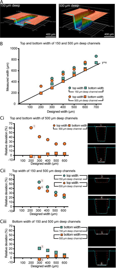
Figure 2.

Quantification of dimensional differences between the device design and the injection molded device (PS device only). (A) Confocal microscope images of channels (designed width = 300 μm; left channel designed height = 150 μm, right channel designed height = 500 μm). The blue line indicates the cross section used for dimension measurements. Measurements of width were made at both the top and the bottom of the channel. (B) Comparison between the average measured width and the designed width for the 150 μm and 500 μm deep channels (the y=x line, representing ideal correspondence between designed and measured values). (Ci-Ciii) Plots of relative deviation for the parameters indicated (left) and corresponding confocal profilometer cross-sections (right). Data points represent the average of three devices produced by the same mold. In all cases, the standard error of the mean was smaller than the symbol plotted; the complete set of raw data is included in the SI, including separately plotted data points for the three replicate devices.
