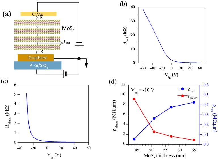
Figure 2.
(a) Schematic diagram for resistances to compose Gr/MoS2/(Cr/Au) vertical field-effect transistor (VFET) with 50 nm-thick MoS2. (b) Vertical Resistance (Rvert) as a function of the back-gate voltage (Vbg) for Gr/MoS2/(Cr/Au) VFET with 50 nm-thick MoS2. (c) Planar resistance (Rplanar) as a function of Vbg for the lateral MoS2 field-effect transistor with 48 nm-thick MoS2. (d) Dependence of and on the thickness of MoS2 channels at Vbg = −10 V.

