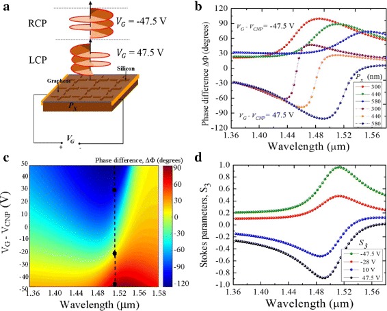
Fig. 7.

a Schematic illustration of the silicon/graphene switching of the polarization state through gate voltage biasing. b. Simulated phase difference as a function of gate voltage biasing. c. Phase difference shown as function of periodicity Px and gate voltage. d. Stokes parameter S3 spectra showing the two states of circular polarization defined by the different gate voltages
