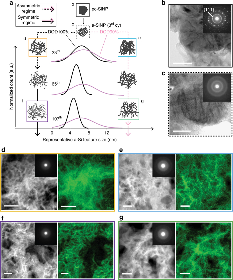
Fig. 5.
Size distribution and electron microscopy images of fully delithiated Si. a Schematics of Si morphological changes over 107 cycles, combined with the Gaussian-fitted size distribution curves of delithiated amorphous-Si (a-Si) for type-A electrodes cycled under depth of discharge (DOD)100% (left) and 90% (right). The distribution curves are stacked with a constant pitch to show the changes over cycles more clearly. Dotted and solid lines show the electrochemical asymmetric and symmetric regimes (Fig. 3h), respectively. The schematics surrounded by different colored squares correspond to the following electron microscopy images. Bright-field TEM images for (b) as-is polycrystalline silicon nanoparticles (pc-SiNP) and (c) porous amorphous SiNP (a-SiNP) after the 2nd cycle. Inset shows the selected area diffraction pattern (SADP) of the imaged area. d–g High-angle annular dark field (HAADF) with SADP inset (left) and electron energy loss spectroscopy (EELS) mapping (right) of delithiated a-Si at (d, e) the 23rd and (f, g) the 107th cycle for (d, f) DOD100% and (e, g) DOD90%, respectively. All scale bars are 50 nm. Combining the results from HAADF and EELS, the feature size distribution for DOD100% becomes much narrower compared to that for DOD90% after the 65th cycle. The trend of particle size and distribution is also shown in Supplementary Fig. 15

