Figure 2.
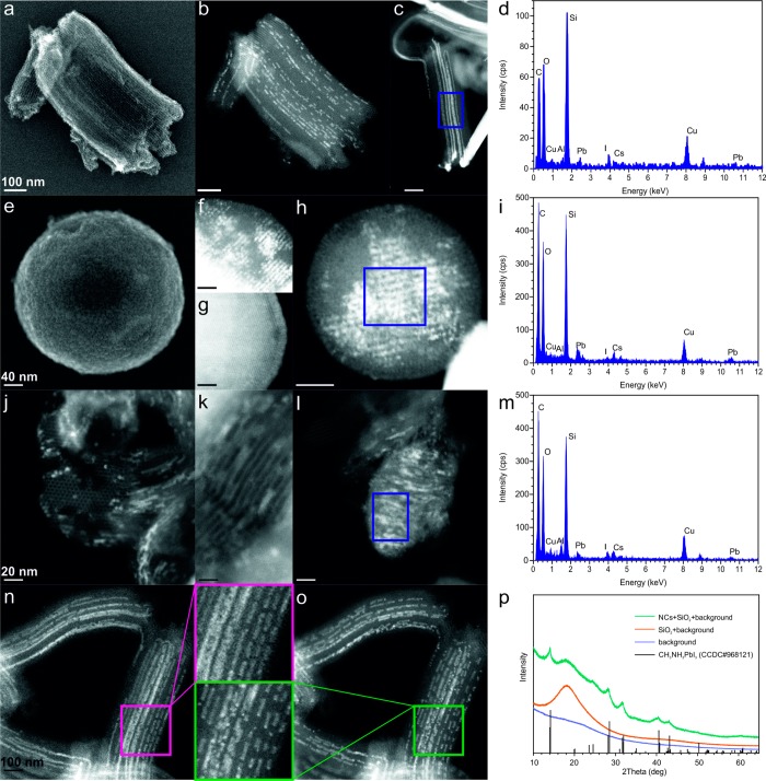
(a) SE-STEM and (b-c) HAADF-STEM images of a 7 nm-SiO2 sample (MSU-H) partially filled with CsPbI3 NCs. (d) EDXS of the area highlighted in (c). (e) SE-STEM and (f, h) HAADF-STEM image of a 4 nm-SiO2 sample (SBA-15) partially filled with CsPbI3 NCs. For comparison, a HAADF-STEM image of pristine 4 nm-SiO2 (SBA-15) is shown in (g). (i) EDXS of the area highlighted in (h). (j-l) HAADF-STEM images of 2.5 nm-SiO2 (MCM-41), partially filled with CsPbI3 NCs. (m) EDXS of the area highlighted in (l). (n-o) HAADF-STEM images illustrating the effect of beam damage on CsPbI3 NCs in 7 nm-SiO2 (MSU-H) during (n) short and (o) long exposures. (p) XRD patterns of 4 nm-SiO2 (SBA-15) impregnated with MAPbI3 NCs, along with reference patterns of the background, pristine template and bulk MAPbI3 (from the Cambridge Crystallographic Data Centre (CCDC) database).

