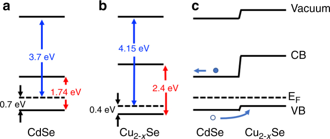
Fig. 5.

Flat band schemes. Energy levels of the CdSe (a), Cu2−xSe (b), and of the heterojunction (c) as obtained from ultraviolet photoelectron spectroscopy (UPS) data (see Supplementary Figure 8) and the bulk band gap values. Energies of Fermi level to vacuum are stated in blue, valence band to Fermi level in black, and the band gap in red color. The full and hollow circles in c represent the photoexcited electrons and holes, respectively, and the arrows indicate the charge separation induced by the heterojunction
