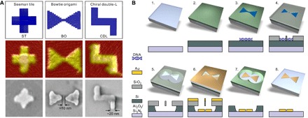
Fig. 1. DNA origami designs, a step-by-step fabrication procedure of the DALI method.

(A) Top: Designed DNA origami shapes (from left to right): ST, BO, and CDL. Middle: AFM images of the folded structures on a mica substrate. Bottom: Scanning electron microscopy (SEM) images of gold nanostructures created by the fabrication method described in detail in (B). The AFM and SEM images are 150 nm × 150 nm in size. (B) Steps of the fabrication procedure. Step 1: A transparent sapphire (Al2O3)/silicon nitride (Si3N4) chip is freshly cleaned by acetone and isopropanol. Step 2: An amorphous silicon layer is grown on top of the substrate by PECVD. Step 3: The substrate is treated by oxygen plasma, after which the DNA origami nanostructures (BO shown here as an example) are drop-casted on the chip. Step 4: The silicon dioxide (SiO2) layer is selectively grown on the bare silicon by CVD, leaving DNA origami–shaped silhouettes in the layer. Step 5: Using the grown SiO2 layer as a mask, the silicon underneath is etched away by RIE. Step 6: The metal is deposited onto the chip using PVD in ultrahigh vacuum. Step 7: The SiO2 layer is removed in a liftoff process using hydrogen fluoride–based wet etching. Step 8: The remaining silicon is removed by RIE, thus leaving the DNA origami–shaped metal nanostructure on the substrate.
