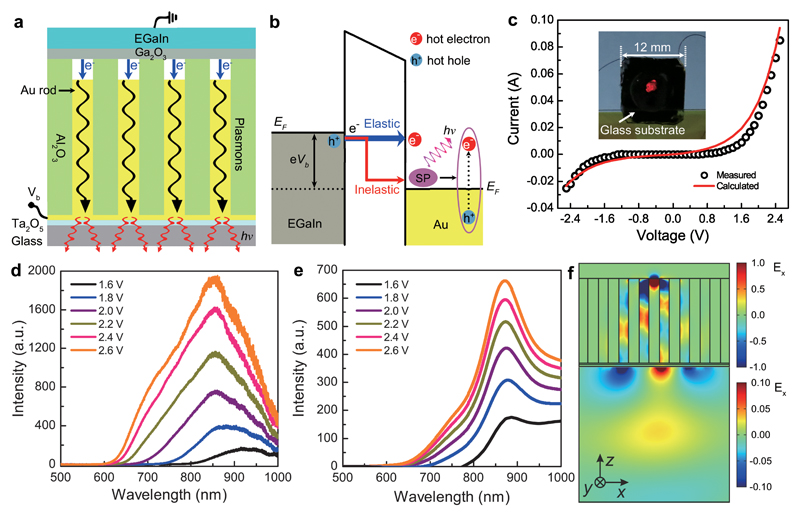
Figure 2. Electrically-driven nanorod metamaterial based on metal-air-metal tunnel junctions.
a,b, Schematics of the device configuration (a) and the tunnelling processes (b). When a bias is applied between the EGaIn and Au nanorods, electrons tunnel across the junctions from occupied states in EGaIn to unoccupied states in Au nanorods. The majority of electrons tunnel elastically to form hot electrons in the Au nanorod tips; the inelastically tunnelling electrons excite surface plasmons in the metamaterial, which can then decay non-radiatively via the excitation of hot carriers or radiatively into photons from the substrate side of the metamaterial. c, Experimentally measured and theoretically calculated current–voltage curves for a device fabricated using the metamaterial shown in Fig. 1. Inset, photograph of the device with an applied bias of Vb = 2.5 V. d,e, Measured (d) and simulated (e) emission spectra of the device as a function of the applied forward bias. f, Simulated near-field map of the metamaterial plasmonic mode excited via tunnelling and the subsequent radiation of the optical signal into the far field.

