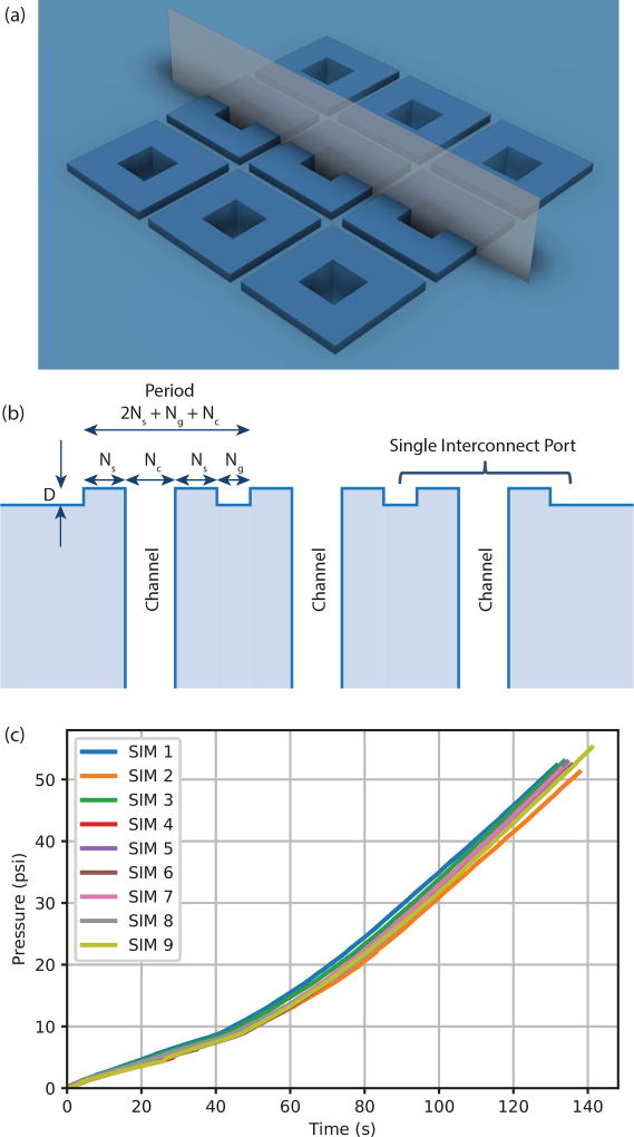
Fig. 4.
SIM design. (a) Integrated square microgaskets printed around each vertical channel on the top surface of a device chip. The top surface is in the XY plane with the Z direction being out of the plane. (b) Schematic illustration of the cross section of the vertical plane indicated in (a). The microgaskets have height D above the surrounding planar surface of the chip. (c) Pressure as a function of time for the test set up in Fig. 1(c) using the device and interface chips in Fig. 2 for each of the 9 chip-to-chip interconnects.

