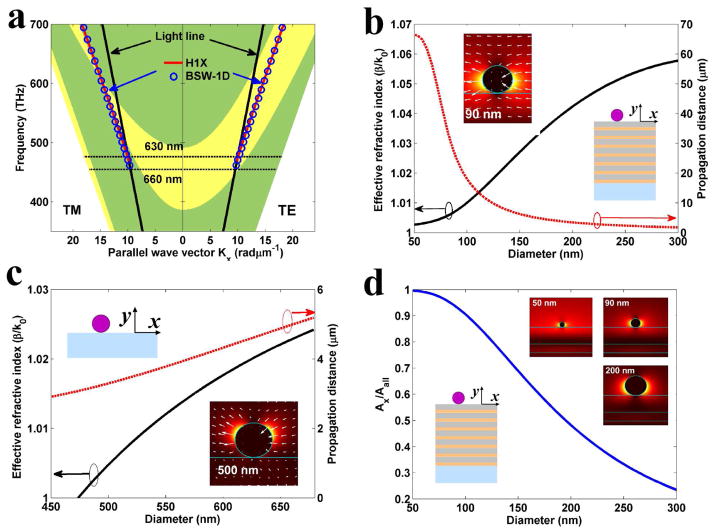
Figure 3. Numerical simulation of the plasmonic mode.
(a) The projected band structure of the dielectric multilayer for TE and TM polarizations. The yellow zone denotes the stop band. The red solid lines and blue circles denote the dispersion relation for H1X mode of Ag NW with diameter 90 nm and BSW-1D mode of polymer NW with diameter 170 nm, respectively. (b), (c) show the effective refractive index and propagation distance of the H1X mode versus the diameter of the Ag NW placed on the DMS (b) or on the glass substrate (c). The incident wavelength was 630 nm. The inset in (b) shows the electric field distribution of the H1X mode for the 90-nm-diameter NW on the DMS. The inset in (c) shows the electric field distribution of the H1X mode of the 500-nm-diameter NW on the glass substrate. The arrows in the inset graphs (electric field distribution) denote the direction of the electric field vectors. (d) The ratio of the electric field energy (Ax/Aall) for the H1X mode versus the diameter. The electric field distributions for H1X mode of Ag NW with diameter 50 nm, 90 nm and 200 nm are shown in the inset, respectively.

