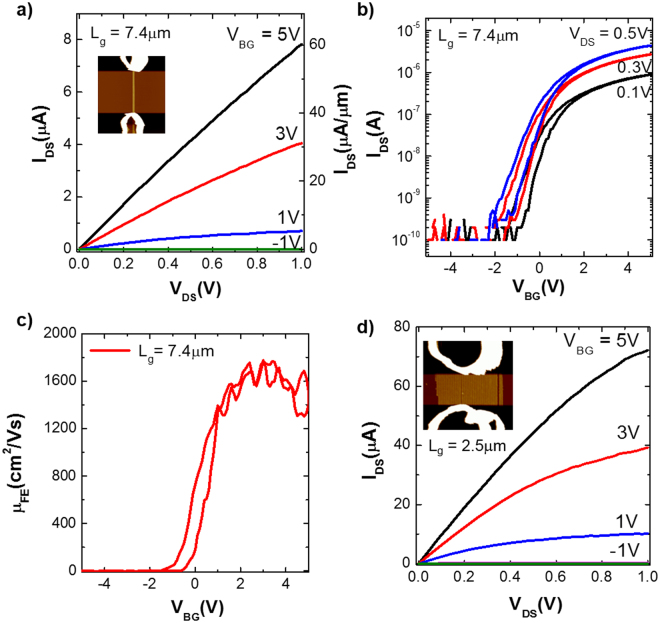
Figure 4.
Electrical characteristics of the back-gated InAs NWFETs. (a) Output (IDS-VDS) and (b) transfer (IDS-VBG) characteristics of the InAs NWFET with a channel length of ~7.4 μm and a total NW width of ~130 nm. The right axis in (a) shows IDS normalized by the total NW width. (c) Field-effect mobility vs. VBG, calculated at VDS = 0.1 V for the same device. (d) The IDS–VDS data of the InAs NWFET with a channel length of high density NW bundles of ~2.5 μm, comprising ~25 NWs.

