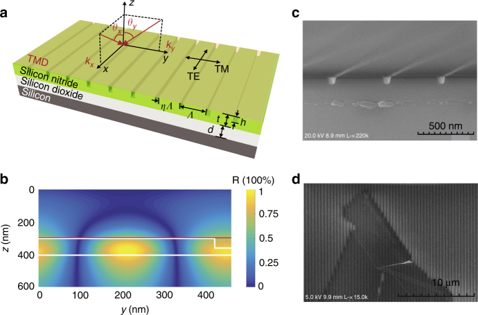
Fig. 1.
The vsWC-PC structure. a Schematic of the 1D PC with a monolayer TMD placed on top. The SiN PC has multiple design parameters, including the period Λ, filling factor η, total thickness t, and the grating thickness h. The SiO2 capping layer has a thickness of d. b The TE-polarized electric-field profile of the PC in the y−z plane. The white lines mark the outline of the PC. The red line marks the position of the monolayer TMDs. c A side-view SEM image of the bare PC. d A top-view SEM image of the TMD laid on top of a PC

