Fig. 1.
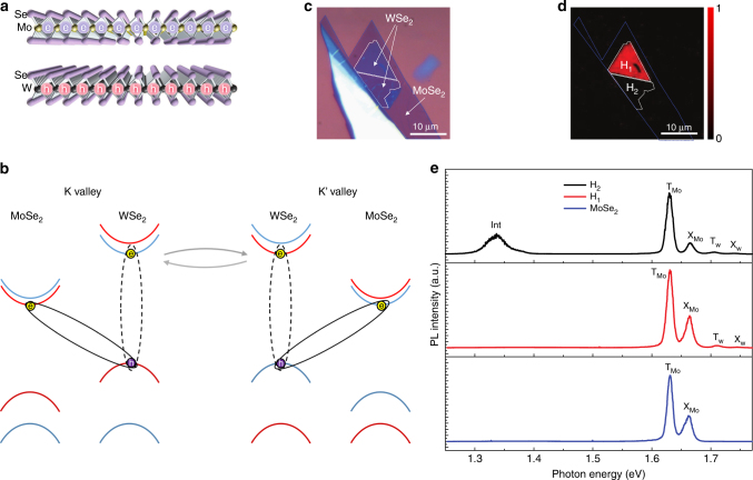
Sample characterization. a MoSe2 and WSe2 form a 2D heterostructures, where electrons are confined in one layer and holes are confined in the other layer. b Schematic of the interlayer exciton and dark exciton. The interlayer excitons are illustrated as solid black ellipses. The dark excitons are represented by the dashed ellipses. Red (blue) curves denote spin-up (spin-down) in the conduction and valence bands while the gray arrowed curves denote the dark exciton valley scattering. c Optical microscope image of the MoSe2/WSe2 heterostructure. Blue dashed line shows the area of MoSe2. White dashed lines show the region of heterostructure, which is separated into two areas labeled as H1 and H2 in d. d Fluorescence image taken with a color camera under white light excitation. It shows a bright (H1) and dark (H2) state in the two different place of heterostructure. e Photoluminescence in the monolayer MoSe2, heterostructure H1 region, and heterostructure H2 region under a 633 nm laser excitation. Peaks on MoSe2 are attributed to exciton (XMo) and trion (TMo) of MoSe2. In H1 area, another two weak peaks appear and are labeled as exciton (XW) and trion (TW) from WSe2. In H2 area, another peak around 1.34 eV emerges, which is attributed to interlayer exciton and labeled as Int

