
Fig. 2.
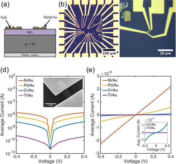
(a) Cross sectional schematic of device structure. Two nanoribbons with different contact configurations are shown. (b) Optical microscope image of a sample with many contact test structures patterned in one area and (c) a higher magnification image of a nanoribbon with four contacts. Average I–V sweeps for each contact metallization with 1 μm channel spacing on a (d) log and (e) linear scale, showing ohmic and semi-ohmic behavior for Pd/Au and Ni/Au contacts, and Schottky behavior for Cr/Au and Ti/Au contacts. Inset in (d) is an SEM image of a two contact Ni/Au device.