
Figure 1.
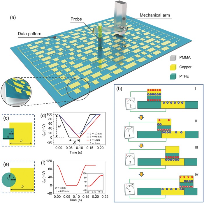
The setup of the TEDS and its working principle. a) Structure of the TEDS with the strip‐shaped surface patterns. b) Charge distribution as the probe scans across a unit pattern. c) Top‐down view of a square‐shaped probe and a unit pattern. d) Analytically calculated voltage signal. e) Top‐down view of a round‐shaped probe and a unit pattern. f) Analytically calculated voltage signal.