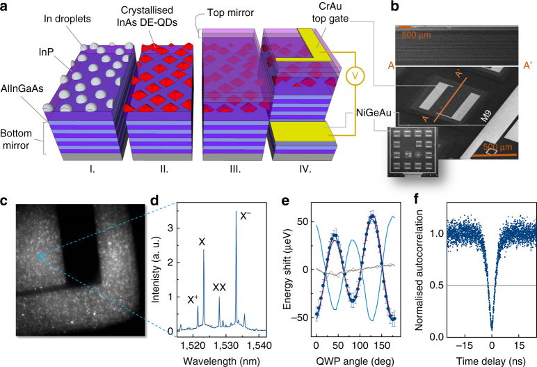
Fig. 1.
Device and dot characterisation. a Growth and fabrication stages of the device, where In droplets are deposited on an intrinsic InP layer grown on a 20-repeats doped Bragg mirror (I.), crystallised under As flux (II.) and overgrown by an intrinsic InP layer followed by a 3-repeats Bragg reflector (III.). Finally, mesas are wet-etched and the doped layers gated (IV.). b SEM image of a typical device mesa, with a cross-section through a mesa and a device overview shown in top panel and inset, respectively. The scale bars give 500 μm for the main panel and 2 μm for the top panel. c Image of the glowing device taken with an InGaAs camera. The bright spots are individual QDs. d Spectrum of the QD circled in c with exciton (X), biexciton (XX), positively charged exciton (X+) and negatively charged exciton (X−) labelled. The broad, low-intensity features show the influence of phonon interaction at 44 K35. e Energy shift of the X (red curve), XX (light blue curve), X+(light grey curve) and X− (grey curve) transitions as a function of quarter wave plate (QWP) angle (see main text). The transition energy at each QWP angle was determined as the centre energy of a Gaussian fit to the spectrum. The solid blue dots are the systematic shift-corrected X data points, with the error bars giving the SD derived from the covariance matrix of the Gaussian fit. The solid blue line gives the result of a fit to the QWP model described in Methods. f Second-order autocorrelation measurement performed on the X line in c

