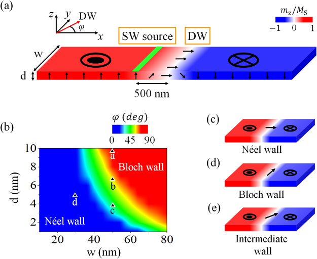
Figure 1.
(a)Schematics of the sample geometry for simulation. The nanostrip is 4 µm long, with a domain wall located at the center, and a spin wave source 0.5 µm to the left. (b) Phase diagram of the equilibrium DW structure for width w ranging from 10 to 80 nm and thickness d from 1 to 10 nm. The structures of the DW correspond to (c) the Néel wall (center magnetization azimuthal angle φ = 0 or 180° to the x axis in the xy plane), (d) the Bloch wall (φ = 90 or 270°), and (e) an intermediate wall.

