Fig. 3.
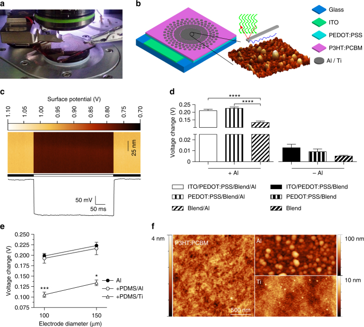
Optimization of the photovoltaic pixel. a Picture of the KPFM measures. b Sketch of the fabricated device. Glass substrates have been coated with a thin film of ITO (200 nm), a thin film of PEDOT:PSS (50 nm), a thin film of P3HT:PCBM (100 nm), and last aluminium (100 nm) or titanium (150 nm). c Representative KPFM map on a Glass/PEDOT:PSS/Blend/Al device obtained by repeating a line scan of 100 nm (vertical direction). The horizontal bar indicates period of dark (black) and light (white). The bottom panel shows the average potential fluctuation during time; each point is the average potential in a single line scan. d Surface potential variations (voltage in light—voltage in dark) for 6 different architectures. Each bar is the mean (±s.e.m.) of at least N = 3 devices, in which at least n = 3 electrodes/points has been measured and averaged. ITO/PEDOT:PSS/Blend/Al: 0.2106 ± 0.0092 V, N = 5, n = 3; PEDOT:PSS/Blend/Al: 0.2259 ± 0.0085 V, N = 5, n = 3; Blend/Al: 0.1334 ± 0.0090 V, N = 3, n = 3; ITO/PEDOT:PSS/Blend: 0.0128 ± 0.0032 V, N = 3, n = 3; PEDOT:PSS/Blend: 0.0091 ± 0.0025 V, N = 3, n = 4; Blend: 0.0052 ± 0.0007 V, N = 3, n = 4. One-way ANOVA, p < 0.0001, F = 177.9. e Surface potential variations with/without a bottom PDMS layer and with Al or Ti top contacts of 100 and 150 µm in diameter. Each point is the mean (±s.e.m.) of at least N = 3 devices, in which at least n = 3 electrodes has been measured and averaged. PEDOT:PSS/Blend/Al-100 µm: 0.1984 ± 0.0043 V, N = 3, n = 3; PEDOT:PSS/Blend/Al-150 µm: 0.2232 ± 0.0082 V, N = 3, n = 3; PDMS/PEDOT:PSS/Blend/Al-100 µm: 0.1927 ± 0.0115 V, N = 5, n = 3; PDMS/PEDOT:PSS/Blend/Al-150 µm: 0.2163 ± 0.0150 V, N = 5, n = 3; PDMS/PEDOT:PSS/Blend/Ti-100 µm: 0.1055 ± 0.0063 V, N = 3, n = 6; PDMS/PEDOT:PSS/Blend/Ti-150 µm: 0.1342 ± 0.0068 V, N = 3, n = 3. f Representative AFM images of PEDOT:PSS/Blend, PEDOT:PSS/Blend/Al, and PEDOT:PSS/Blend/Ti surfaces

