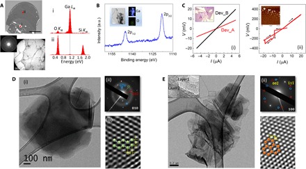
Fig. 4. Characterization of gallenene films.

(A) Top: SEM image of the gallenene sheet on the SiO2 substrate. Scale bar, 50 μm. The EDS spectrum collected from the bulk region (i) shows a strong Ga L peak, whereas the spectrum of the thinner region (ii) also shows this peak but with much reduced intensity. Bottom: The TEM image of this transferred film along with SAED showing that these Ga films are crystalline. Scale bar, 2 μm. (B) XPS data showing two intense peaks at binding energies of 1117.0 and 1143.0 eV, which correspond to 2p3/2 and 2p1/2 states, respectively, of metallic Ga. Inset: Composition mapping of Ga films in TEM showing the presence of Ga with negligible amount of O. Scale bar, 100 nm. a.u., arbitrary units. (C) (i) I-V characteristics of two gallenene devices. The inset shows the optical image of Dev_B. Scale bar, 15 μm. (ii) I-V curve showing breakdown of gallenene device at higher currents. The insets show the AFM image of the Ga film after breakdown. (D and E) Representative bright-field TEM images (i) along with SAED patterns (ii) and HRTEM image (iii) for the gallenene b010 and a100 sheets, respectively. The simulated crystal structure for these two orientations is superimposed on the HRTEM images. Scale bar, 200 nm.
