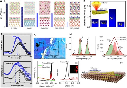
Fig. 5. Substrate effects on gallenene.

(A) Charge accumulation and depletion of gallenene a100 on Si, Ag, GaN, and SiO2 substrates. Charge accumulation and depletion of gallenene b010 on the SiO2 substrate are shown in the rightmost panel. The accumulation and depletion of charge are shown in pink and green. Top and bottom rows represent top and side views of the structures. The charge uniformly accumulates at the interface of gallenene and metallic substrates, whereas the charge accumulates at the Si (Ga) and Ga bond for Si (GaN) and SiO2 substrates. This implies that the interaction between gallenene and the metallic substrate is nondirectional toward metallic bonding, whereas the interaction between gallenene and semiconductors (GaN, Si, and SiO2) is toward covalent bonding. The bars represent the interlayer binding energy (Eb) per Ga atom between gallenene and the substrate. The larger value of binding energy indicates the greater interaction between gallenene and the substrate. Blue, yellow, cyan, brown, purple, and red spheres are Ga, Si, Ag, Ga (in GaN), N, and O atoms, respectively. Dotted purple line represents the unit cell of the structure. The iso-surface value is set to ~0.002 (e/Å3). (B) Relative interaction (adhesive force) of gallenene with substrates (Si, Ag, SiO2, and GaAs) as measured using indenter. (C) Top: Absorption spectra of bulk Ga and ultrathin gallenene sheets. Bottom: Absorption spectra of gallenene sheets on two different substrates, SiO2 and GaAs. (D) (i) Optical micrograph of gallenene sheet on MoS2. Scale bar, 20 μm. Raman (ii) and PL (iii) spectra of pristine MoS2 and MoS2 underneath gallenene are shown. The PL map of the region indicated by dashed lines in (i) is shown in the inset. (iv) The XPS spectra for the MoS2 region underneath Ga are shown, indicating the evolution of 1T phase of MoS2. (v) Schematic illustrating the idea.
