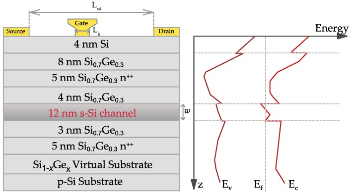
Figure 2.
(Left) Cross section of the Si/SiGe MODFETs showing the vertical layout of the transistor with a schematic of the contacts; the strained-Si layer of thickness w is highlighted. (Right) A plot of the vertical profiles of both bands edges and the Fermi level under the gate in equilibrium is given; the double-deck supply layer structure leads to a double electron channel in the quantum well [32].

