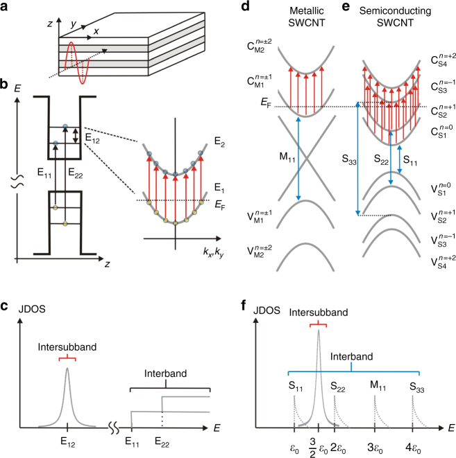
Fig. 1.
Schematic illustrations of allowed intersubband and interband transitions in semiconductor quantum wells and carbon nanotubes. a A quantum well made from a heterostructure of two semiconductors (white and gray) with different band gaps. b Intersubband (E12) and interband (E11 and E22) transitions in a quantum well. E12 is allowed only for incident light polarized along the quantum-confinement (z) direction and only when the system is doped (n-doped in the present case). c The joint density of states (JDOS) for the intersubband and interband transitions in a quantum well. Interband transitions (blue arrows) and intersubband transitions (red arrows) in d metallic and e semiconducting carbon nanotubes. See the text for the selection rules applied to these transitions. f The JDOS for the intersubband and interband transitions in carbon nanotubes. Here, ε0 = 2γ0aC − C/dt, γ0 is the nearest-neighbor transfer integral for graphene, aC − C is the nearest neighbor C-C separation in graphene, and dt is the nanotube diameter

