
Figure 1.
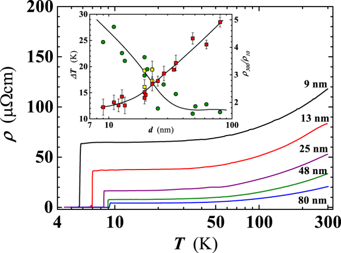
Temperature dependence of the resistivity for selected Nb films, with a thickness ranging from 9 nm to 80 nm. Inset: width of the plateau region (ΔT), above TC, as a function of d (circles). As ΔT we have considered the T interval corresponding to a film resistivity change of ±2.5% of ρ(T) @ 10 K. Squares: resistivity ratio at T = 300 K and at T = 10 K as a function of d. All films have been deposited on SiO2 substrates except those, shown by yellow filled symbols, deposited on sapphire.