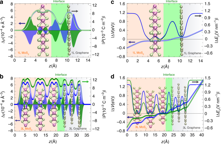
Fig. 4.
Asymmetric dipolar contributions at the MoS2/Graphene interface. a, b Induced charge density (left y-axis) and electric polarization (right y-axis) for 1L MoS2/1L Graphene and 3L MoS2/3 L Graphene, respectively. The applied electric field is ±1.0 V nm−1. Blue (green) curves correspond to positive (negative) fields. Positive (negative) fields go towards graphene (MoS2), and vice versa. The MoS2/Graphene interface is highlighted to show the unbalanced formation of electric dipole moments between graphene and MoS2 accordingly with the number of layer layers used to form the heterostructures. (c-d) Difference in electrostatic potential in the slabs with and without the external electric field of ±1.0 V nm−1, and their corresponding response field for 1L MoS2/1L Graphene and 3L MoS2/3L Graphene, respectively. The absolute values of and are taking in (c) and (d) for comparison at the same side of the plot. Geometries for all systems are highlighted at the background of each panel in opacity tone

