Fig. 6.
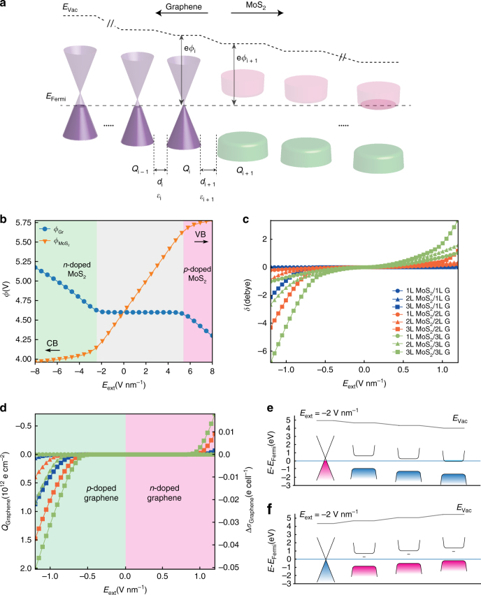
Classical electrostatic approach for charge redistribution of MoS2/Graphene vdW heterostructures. a Schematic band diagram of the multilayer MoS2/Graphene heterostructures. Vacuum level (Evac), work function (), surface charge density (Qi), interlayer distance (di), and relative permittivity (εi) are shown for each stacking i. b Work functions of graphene and MoS2 as functions of external electric field Eext (V nm−1). The regimes of the n-doped and p-doped MoS2 are highlighted in green and faint red, respectively. The Fermi level reaches the conduction band (CB) or valence band (VB) of MoS2 when large negative or positive Eext is applied, relatively (as shown by the arrows). c Electric dipole moment δ (Debye) as a function of Eext (V nm−1) for different number of graphene and MoS2 layers on the heterostructures. d Surface charge density QGraphene (left axis) and the amount of charge transfer between graphene and MoS2 layers ΔσGraphene (right axis) as a function of Eext (V nm−1) for different MoS2/Graphene systems. The curves follow the labeling in (c). e–f Band alignments for an illustrative case, e.g., 3L MoS2 /1 L Graphene under −2.0 V nm−1 and +2.0 V nm−1 electric fields, respectively. Positive charges are shown in faint red and negative charges are shown in blue, respectively. Only band structures near the Fermi level are shown for illustration

