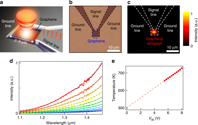
Fig. 1.
Device structure and emission from a graphene device under DC bias. a A schematic illustration of graphene blackbody emitter. Square graphene sheet on a SiO2/Si substrate is connected to source and drain electrodes (signal and ground lines). Modulated blackbody emission is obtained from graphene by applying input signal. b An optical-microscope image of the graphene emitter with a coplanar waveguide. Blue and black dashed lines indicate square graphene sheet and the coplanar electrodes, respectively. c IR camera image of the thermal emission at Vds = 4 V for the emitter shown in (b). The bright emission is localized to a small hotspot in graphene. d Emission spectrum from a single-layer graphene emitter for Vds = 5.5–8 V with steps of 0.25 V. The small peaks located at wavelengths around 1.4 μm are due to the light absorption by water in air and remain even after spectral correction (see Methods). The gray broken curves are fitting results based on Planck’s law. e Graphene temperatures obtained by the Planck’s-law fittings in (d). Their temperatures depend linearly on the applied voltages

