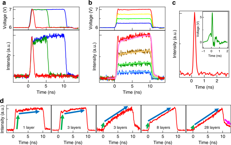
Fig. 2.
Experimental high-speed light emissions. Time-resolved emission under a rectangular bias voltage with a different pulse widths (1, 5, and 10 ns in width and 6 V–7 V in height) and b different pulse amplitudes (10 ns in width and 6 V–6.25, 6.5, 6.75, and 7 V in height) to single-layer graphene device. c Very-short-pulsed light generation with a width of 200 ps for three-layer graphene device (red curve) by applying a pulsed input voltage with a width of 100 ps and amplitude of 0–6 V (green curve). d Time-resolved emission for the emitters with single, three, eight, and 28-layers graphene. The emission responses consist of two components: an initial fast response with a rise time of ~100 ps (green arrows) and a second slow response of the temperature rise (blue arrows), whose intensity ratios roughly depend on the number of graphene layers. For thick graphene, the slow fall component of the emission is observed as shown by pink arrow

