Fig. 5.
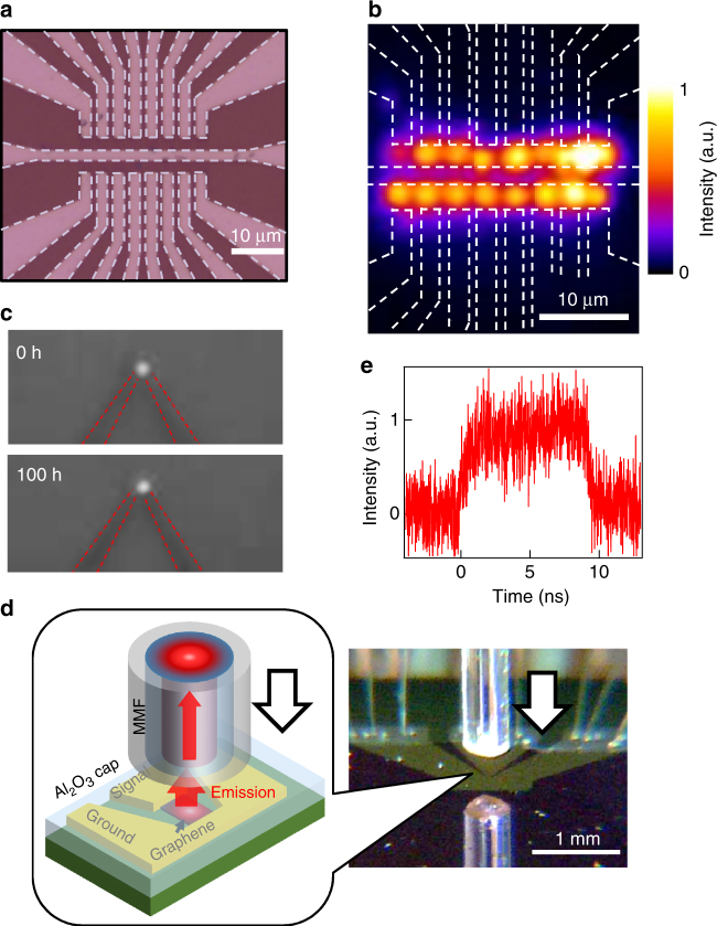
Highly integrated graphene emitters. a An optical image of the fabricated device of the 2 × 8 array emitters, whose size and pitch are 2 × 2 μm and 3 μm, respectively. Dashed lines indicate Pd electrodes. b NIR camera image of the emission for the array device at Vds = 10 V. All devices are connected to the same voltage source, but an adjustable series resistor is introduced for every emitter to equalize the emission intensity of every emitter. c NIR camera images of the light emission from Al2O3-capped emitters with three-layer graphene after 0 and 100 h of continuous work in air. No significant change is observed after 100 h. d Optical image of the direct coupling of the capped light emitter to the multimode optical fiber (MMF) in air. In this picture, MMF is approaching the emitters. Inset: schematic image of the direct coupling of a capped light emitter to a MMF. e High-speed light emission measured by the direct coupling shown in (d)

