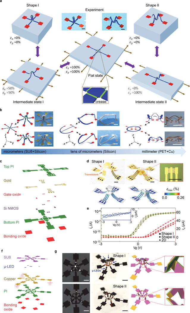
Figure 1. Morphable 3D mesostructures and integrated circuits by loading-path controlled mechanical assembly.

a, Conceptual illustration of the strategy through a sequence of FEA results and a pair of colorized SEM images of two 3D mesostructures. b, 2D shapes, FEA predictions and corresponding experimental images (SEM or optical) of morphable 3D mesostructures with diverse materials and length scales [left: bilayers of SU8 (1 μm at the creases and 2 μm at the other regions) and Si (50 nm); middle: Si (1.5 μm); right: bilayers of PET (50 m) and Cu (1 m)]. Shape I (upper frames) corresponds to simultaneous release and Shape II (lower frames) corresponds to sequential release (y direction first, and then x direction). Scale bars, 50 μm for the left panel; 500 μm for the middle panel; and 5 mm for the right panel. c-e, Design of a morphable 3D structure that embeds several silicon transistors, along with metal interconnects. c, The exploded view of the 2D geometry. d, Optical images of two configurations of the structure after 3D assembly. Shape I and Shape II correspond to simultaneous and sequential release, respectively. Scale bars, 200 . e, Current-voltage (I-V) characteristics of a transistor measured with the structure in Shape I, Shape II and the planar state. The color in the FEA results of d corresponds to the magnitude of maximum principal strain in the metal. f and g, Design for a morphable 3D optoelectronic device that incorporates four μ-LEDs. The left shows an exploded view of the 2D geometry, and the right shows optical images and modeling results for two device configurations (Shape I and II). Scale bars, 1 mm.
