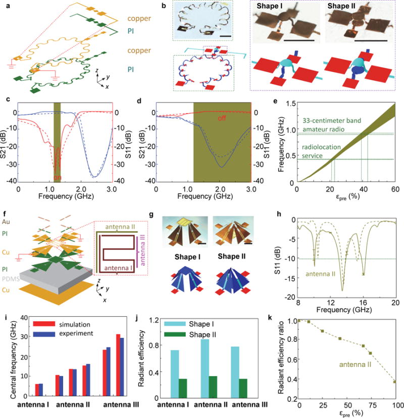
Figure 5. Applications of 3D morphable mesostructures as switchable radio frequency (RF) electronic components.

a-e, A morphable RF circuit. a, Exploded view illustration of the layer construction [Cu (3 m), PI (2 μm)]. b, FEA predictions and optical images of the overall device, and magnified view of the capacitor structure that results from different release sequences. Shape I and II result from simultaneous and sequential release (x direction first, and then y) of the elastomer substrate, respectively. Scale bars, 1 mm. c, Measured and simulated S21 and S11 versus frequency for Shape I, when the device is formed from a biaxial prestrain (εx-pre = εy-pre = 60%). d, Measured and simulated S21 and S11 versus frequency for Shape II, when the device is formed from a biaxial prestrain (εx-pre = εy-pre = 60%). e, Simulated switchable frequency band as a function of the prestrain, when the device is subject to different biaxial prestrains. f-i, A morphable electromagnetic device with shielding capability. f, Exploded view of the layer construction [thickness of each layer from top to bottom: Au (100 nm), PI (1.5 μm), Cu (9 m), PI (12 m), PDMS (5 mm), Cu (100 nm)]. g, FEA prediction (lower frames) and optical images (upper frames) of the device. Scale bars, 5 mm. h, Measured and simulated dependence of the return loss (S11) on the frequency for antenna II. i, FEA predictions and experimental measurements of the central frequency for antenna I, II and III. j, Simulated radiant efficiency for antenna I (at frequency f=6.0 GHz), II (f=13.58 GHz) and III (f=23.2 GHz) when the device is released from a biaxial prestrain (εx-pre = εy-pre = 85%). k, Simulated radiant efficiency ratio for antenna I (f=6.0 GHz) as a function of the prestrain. In c, d and h, the solid and dash lines correspond to the experiment and simulation results, respectively.
