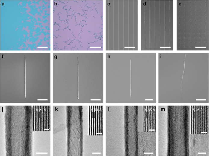
Fig. 2.
Transition metal dichalcogenide (TMD)-nanoscrolls (NSs) from self-scrolling chemical vapor deposition (CVD)-based TMD monolayer flakes. a Optical image of CVD-grown MoS2 monolayer flakes on a SiO2/Si substrate (the purple area represents the substrate, the green area represents the MoS2 monolayers; scale bar, 500 μm). b Optical image of MoS2-NSs on a SiO2/Si substrate (scale bar, 100 μm). c–e The fabrication process of a MoS2-NS array (scanning electron microscopy—SEM image shown, scale bars, 50 μm). c Large-area MoS2 monolayer film patterned into ribbons by focused ion beam (FIB) etching (the dark region represents MoS2 film, the bright area is bare substrate). d Long MoS2-NSs made from the controllable scrolling of the patterned MoS2 film in c. (The white parallel lines are MoS2-NSs, and the dark area represents the substrate). e A 12 × 6 array of MoS2-NSs fabricated via a second FIB etching of the long MoS2-NSs in d. f–i SEM images of typical TMD-NSs on SiO2/Si substrates: MoS2-NSs (f),WS2-NSs (g), MoSe2-NSs (h), and WSe2-NSs (i). (Scale bars, 5 μm in f, i and 10 μm in g, h). j–m TEM images of typical TMD-NSs: MoS2-NSs (j),WS2-NSs (k), MoSe2-NSs (l), and WSe2-NSs (m). (Scale bars, 20 nm). Inset: High-magnification images of sidewalls of TMD-NSs (scale bars, 2 nm)

