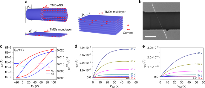
Fig. 4.
Electrical characteristics of MoS2-NSs (nanoscrolls). a Schematic representations of current conduction in transition metal dichalcogenide (TMD)-nanoscrolls (NSs), TMDs monolayer, and TMDs multilayer under bias. The W represents the conduction channel width. The NSs made from the below TMDs monolayer have a much shorter W. For TMDs multilayer, the current only passes through the outermost shell layers. b SEM image of a typical MoS2-NS FET (scale bar, 10 μm). c Transfer characteristics of MoS2-NS tested in N2 (red) and air (blue). d Output characteristics of MoS2-NS tested in N2. e Output characteristics of MoS2-NS tested in air

