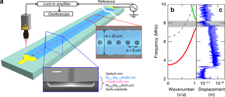
Fig. 1.
1D phononic crystal waveguide. a A schematic of the PnC WG and the measurement setup. The bottom inset shows SEM image of the cross-section of the device which is composed of a GaAs/AlGaAs heterostructure fabricated by selectively etching the Al0.65Ga0.35As layer, scale bar is 5 μm. The periodic structures are determined by the WG width of 22 μm and the hole pitch of 8 μm as shown in the right inset (false colored SEM image). The nanomechanical vibrations are piezoelectrically excited at the right edge and detected at the left edge with a laser Doppler interferometer at room temperature and in a high vacuum (2 × 10⁻⁴ Pa). b The FEM simulated dispersion relation of the PnC WG. The internal stress between the GaAs and Al0.27Ga0.73As layers is included in the simulation34. The dashed line indicates the second phonon band, which does not contribute to the transmission due to the piezoelectric transducer electrodes being located at the nodal position of the mode in this band. c The experimental transmission spectrum, which is measured at the left edge by employing continuous excitation with 1.0 Vrms from the right edge

