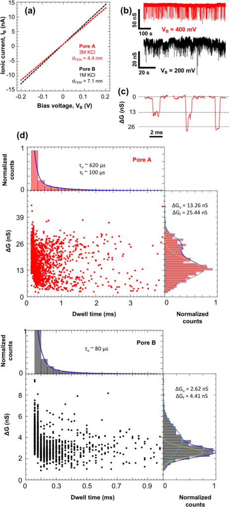
Figure 5.
Double-stranded DNA translocation through WS2 nanopores. (a) Current–voltage measurement of WS2 nanopores with diameters (dTEM) of (i) 4.4 ± 0.9 nm (pore A in red) and (ii) 7.1 ± 0.5 nm (pore B in black), yielding open pore conductances of 61.01 nS and 69.86 nS, respectively. (b) Ionic conductance time trace of DNA translocation events through the nanopore devices shown in (a) with 10 ng/µL of 15 kbp dsDNA at VB = 400 mV for pore A and VB = 200 mV for pore B filtered at 10 kHz. (c) Zoomed-in events illustrating unfolded, partially folded, and folded (left to right) DNA translocation events with the open pore conductance subtracted for pore A. (d) Scatter plots of change in conductance vs event duration for (i) 1890 events (pore A) and (ii) 2030 events (pore B). The histogram on the right shows the change in conductance fitted with two Gaussian curves for unfolded (ΔGu, yellow) and folded events (ΔGf, cyan). The histogram on the top shows the event duration or dwell time fitted with two exponential decay curves for unfolded (τu) and folded (τf) events. The τf was not obtained for pore B as we were limited by the sampling rate of the current amplifier.

