Figure 6.
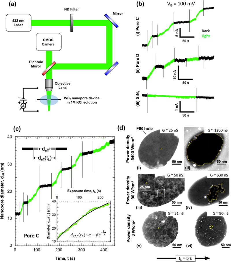
Optical activity of WS2 nanopores in 1 M KCl solution. (a) Schematic of the optical measurement setup. A 532 nm (green) laser is focused onto a nanopore device using an objective lens (4×) and 3-axis micromanipulator stage. The positions of the laser and SiNx window are monitored with a CMOS camera, while its power is controlled through a variable neutral density filter and the laser driving voltage. All measurements were performed in 1 M KCl solution. (b) Change in ionic current through WS2 and SiNx nanopores with laser exposure. Ionic current (IB) measurements at VB = 100 mV were obtained for two WS2 nanopores of effective diameters (deff) of (i) 11.1 nm (pore C) and (ii) 43.2 nm (pore D) and a SiNx nanopore with (iii) deff = 4.8 nm. Periods when the laser (power density = 3 W/cm2) is turned on (light) and off (dark) are represented in green and black, respectively. The spikes in IB correspond to the capacitive noise from switching the laser on or off. (c) Change in effective diameter of pore C with time. The effective diameter (deff) was plotted against the experiment time, t. The regions with the laser on (green) were extracted and concatenated into a single plot (inset) as a function of exposure time, tL. The resulting exponential fit for the relation between effective nanopore diameter and laser exposure time is given by α = 55.1 nm, β = 43.5 nm, and γ = 249.5 s. An illustration of the expansion of the pore is shown on the top left. (d) STEM observation of the laser-induced expansion of nanopores. STEM images were obtained of WS2 nanopores (outlined in yellow) with initial diameters (dTEM) of (i) 4.6, (iii) 4.0, and (v) 4.0 nm. Images after laser exposure (tL ~ 5s) to power densities of (ii) 5400, (iv) 90, and (vi) 3 W/cm2 at VB = 0 V show expansion of pores. Corresponding conductance values before and after exposure are also provided.

