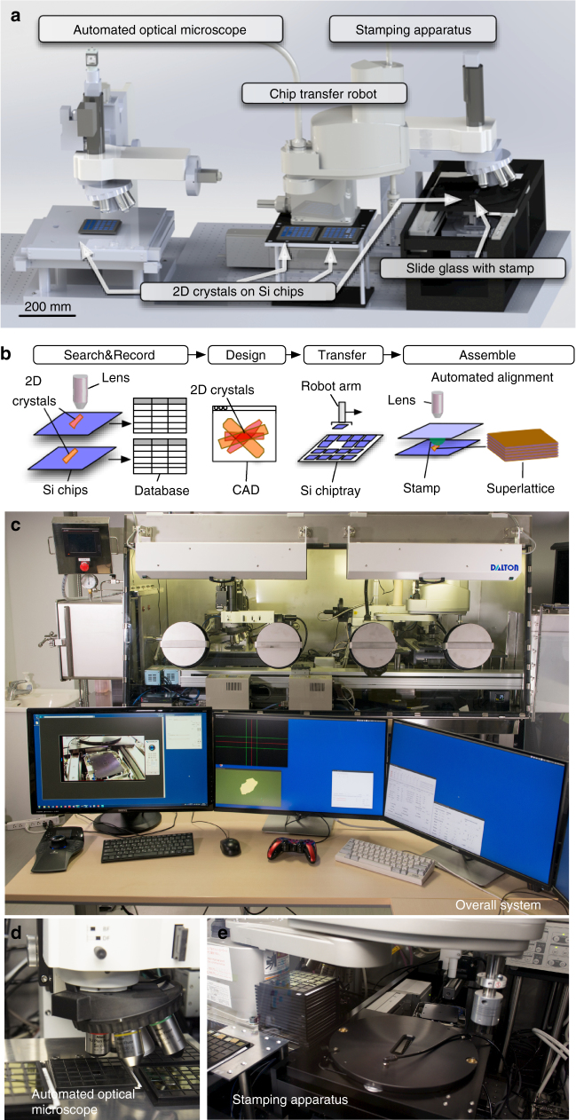
Fig. 1.
The computer-assisted design schematics, functionalities, and photographs of the system. a Computer-assisted design schematics of the presented robotic system comprising an automated optical microscope, stamping apparatus, and Si chip transfer robot. b Schematics of the vdW heterostructure fabrication process. First, the automated high-speed optical microscope with motorized XY scanning stage scans the surfaces of SiO2/Si chips. When 2D crystals are detected, their positions and shape parameters are recorded in a database. By using customized CAD software, the combination, relative positions, and crystallographic orientations of the 2D crystals are designed. Finally, robots directed by the computer-vision algorithm assemble the vdW heterostructures layer by layer onto a polymer stamp through the vdW force. c–e Photographs of c entire system, d close up of automated optical microscope, and e stamping apparatus

