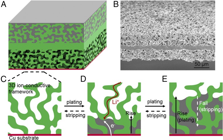
Fig. 1.
Schematic for the process of Li plating and stripping in the 3D Li-ion-conductive host. (A) Schematic of the 3D ion-conductive host for studying Li-ion plating/stripping, where the upper layer is filled with the Li source and the lower layer is empty with Cu deposited on the bottom. (B) Side-view SEM image of the pristine 3D ion-conductive host. 2D local schematic for (C) the lower layer of the pristine empty host without Li, (D) Li deposited in the 3D ion-conductive host from the bottom current collector, and (E) more Li deposited and grown in the 3D host.

