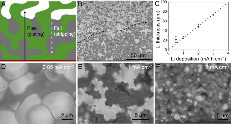
Fig. 4.
Li plating/stripping behavior in the garnet framework. (A) Schematic of Li rise/fall within the garnet framework during plating/stripping. (B) SEM image of 2 mA h cm−2 of Li deposited in the garnet framework. (C) Evolution of Li deposition thickness with the areal capacity of deposited Li. Cross-sectional SEM images of Li deposited in garnet framework at different current densities: (D) 0.05 mA cm−2, (E) 1 mA cm−2, and (F) 2 mA cm−2.

