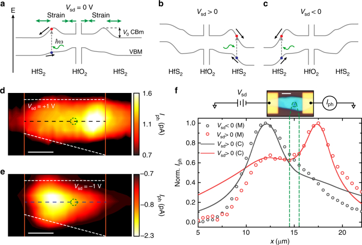
Fig. 4.
Charge funnel effect in HfS2/HfO2 engineered devices. a Schematic band diagram of a device subject to strain induced by local oxidation, with Vsd = 0 V, according to the proposed geometry in Fig. 1. b, c Schematic band diagrams of the device under Vsd > 0 and Vsd < 0, respectively. d, e SPCM map of the device under Vsd = ±1 V, respectively. SPCM maps were acquired using λ = 473 nm, P = 150 W cm−2 at Vbg = +30 V. f Normalised photoresponse along the centre of the channel in the SPCM maps in panels d, e (dots) and simulated curves (solid lines) according to Eq. (1). Inset: optical micrograph of the measured device and measurement diagram. Scale bars are 3 μm

