Fig. 2.
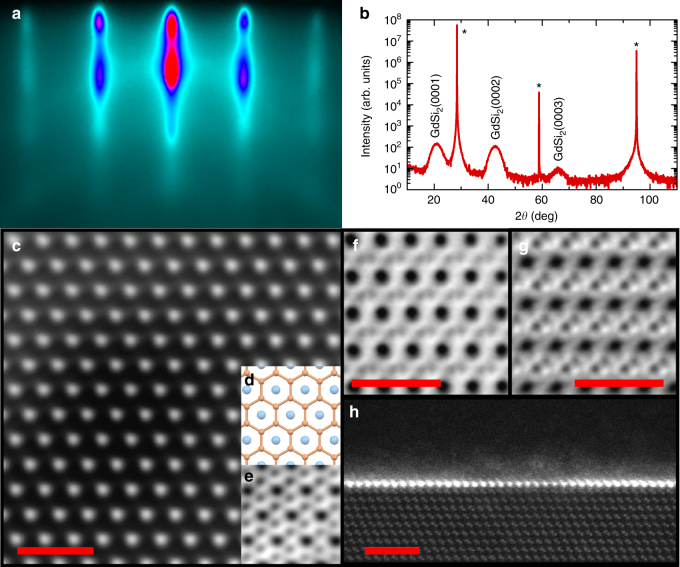
Structural characterization of silicene materials. a RHEED image of 4-5 ML GdSi2 along the azimuth of the Si substrate. b θ-2θ X-ray diffraction scan of 4-5 ML GdSi2 on Si(111). Asterisk denotes peaks from the Si substrate. c Top view of bulk GdSi2 (HAADF-STEM image). d Top view of bulk GdSi2 (ball-and-stick model). e Top view of bulk GdSi2 (BF-STEM image). f BF-STEM image of a GdSi2 cross-section viewed along the [110] zone axis of the Si substrate. g BF-STEM image of a EuSi2 cross-section viewed along the [110] zone axis of the Si substrate. h HAADF-STEM image of 1 ML of GdSi2 on Si(111). Scale bars, c, f, g 1 nm and h 2 nm

