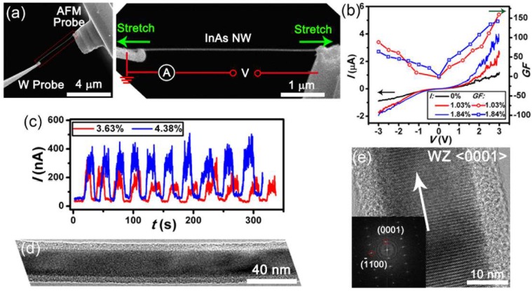
Figure 4.
In-situ scanning electron microscopy (SEM) tensile test in measuring the piezoelectric and piezoresistive effects of InAs NWs. (a) SEM image showing the experimental setup for the electromechanical measurement of InAs NWs; (b) The measured current-voltage (I-V) and gauge factor-voltage (GF-V) curves and (c) the electrical current responses of InAs NWs; (d) The low-magnification and (e) high-resolution transmission electron microscope (TEM) images of the NW measured in (b). Reproduced with permission from [24]. John Wiley and Sons, 2015.

